Webinar Series—
Test Strategies for the Data Explosion
More data, more tests, more measurements. With industry partners, we discuss strategies for higher productivity and accurate results.
Enabling Quantum Advantage: Overcoming Cryogenic I/O Bottlenecks
October 21, 2025 - 9:00am PT
As quantum computing scales toward practical applications, cryogenic I/O systems are emerging as a critical bottleneck. In this joint webinar, FormFactor and Delft Circuits present their roadmaps to address the evolving challenges in cryogenic I/O over the next five years. Building on insights from our previous session, we will explore the increasing complexity of designing and fabricating scalable, high-integrity, and maintainable cryogenic interfaces.
We begin by outlining the current and future requirements for quantum computers, focusing on four key bottleneck categories:
- Physical I/O Scaling – Managing connections across RT, 4K, and mK stages, with emphasis on pre-cooling strategies.
- Signal Integrity – Addressing thermal loads, noise, S-parameters, and crosstalk.
- Modularity & Installability – Ensuring flexible and efficient system integration.
- Reliability & Maintenance – Designing for long-term operability and serviceability.
FormFactor will introduce these challenges from the perspective of a cryostat builder and the limits of scaling traditional chandelier style dilution refrigerators, while Delft Circuits will demonstrate how their technology roadmap aligns with and solves these bottlenecks. Join us to see how this partnership is paving the way for scalable quantum systems and accelerating the path to quantum advantage.

Moderator: Jack De Grave, Director of Business Development, FormFactor Inc.
Jack DeGrave has been an integral part of the FormFactor-HPD Business Development team since early 2021, where he has been instrumental in engaging with Quantum Development Community members to identify and address the needs for cryogenic test and measurement, high-density I/O device interfacing, and cryostats for quantum processor deployment. Jack's expertise in cryogenic test and measurement dates back to his PhD studies at the University of Wisconsin-Madison, where he researched low-temperature transport properties of helimagnets and skyrmions starting in early 2010. Following his graduation, Jack held various business development positions at leading cryogenics companies, accumulating over a decade of experience in cryogenic system design and test & measurement.

Speaker: Joe Yeager, Quantum Application Specialist, FormFactor Inc.
Joe Yeager is a seasoned quantum and cryogenics application specialist at FormFactor, where he has been contributing his expertise for the past two years. With over two decades of experience in cryogenics and low temperature physics, Joe provides unparalleled support for the company's cryogenic test and measurement solutions. He earned his PhD from Kent State University and further honed his skills as a postdoctoral researcher at NASA Goddard Space Flight Center. Joe's extensive technical knowledge is complemented by his experience in account and product management, having held sales and marketing roles at Lakeshore Cryotronics, Oxford Instruments, and Agilent Technologies.

Speaker: Brenda Rovers, , Delft Circuits
Brenda Rovers recently joined the Delft Circuits Communication and Marketing team. After her joint Physics and Science Communication master, she has found a lot of joy in communicating about Quantum hardware for the cable company. Meanwhile she is gathering insights on the impact of quantum technology.
In her spare time, she goes on long walks with her dog, conquers obstacles during survival running, spars during kobujutsu classes and plays bombastic music pieces on the accordion.
ON-DEMAND WEBINARS
A Commercial Implementation of Modal Calibration to Improve GSSG Calibration
Available for on demand viewing
In RF testing, the goal of calibration is to remove the effects of the test setup, including cables, connectors, and adapters, so that the measured results accurately reflect the Device Under Test (DUT) itself. However, performing accurate on-wafer calibrations is challenging, particularly for differential topologies, as the coupling inherent to these precludes accurate measurements unless accounted for. Most traditional RF calibrations do not compensate for this coupling, resulting in inaccurate, and in some cases physically implausible, measurements.
Modal Calibration is one technique to characterise and remove this crosstalk, and is now available, for the first time, in a commercial calibration software.
This webinar will discuss RF calibration techniques, their limitations as applied to differential topologies, and present the Modal Calibration algorithm. Real-world validation results will be demonstrated to illustrate the accuracy improvements which can accrue from its use.
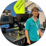
James Hibbert, Principal Applications Engineer, FormFactor Inc.
James is a key member of FormFactor's Centre of Expertise, a group comprised of highly experienced engineers and technical specialists responsible for advancing the frontiers of semiconductor wafer testing and measurement. He is specifically focused on overcoming the challenges of accurately characterising RF devices, particularly for emerging applications such as 6G.
Prior to his tenure at FormFactor, James was an electronics engineer at Fotenix and interned at Broadcom.
He received a doctorate in Electrical Engineering from University of Manchester.
Smarter Probe Station Control with Velox 3.4.5
Available for on demand viewing
Join us for an in-depth look at Velox 3.4.5, the latest release of FormFactor’s probe station control software, packed with enhancements to boost performance, usability, and automation. We will take a look at its useful and efficient features, including advanced probe cleaning capabilities, an upgraded Workflow Guide with new Quick Start workflows, and expanded Autonomous Assistants for RF and High-Power measurements.
We’ll also explore the improved Motorized Positioner Setup for North/South layouts and the new Python 3 scripting environment with preloaded scientific libraries, enabling advanced automation and data analysis right out of the box.
Whether you’re focused on precision probing, streamlined workflows, or automation, this webinar will equip you with the knowledge to leverage Velox 3.4.5 to its fullest potential.
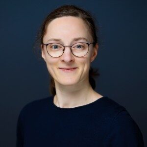
Anja Radke, Applications Training Manager, FormFactor Inc.
Anja Radke is a member of FormFactor’s Centre of Expertise, where she focuses on knowledge-sharing initiatives and best practices for Velox probe station control software. With a background in electrical engineering and business management, she brings nearly 20 years of industry experience to her role—offering practical insights that help users get the most out of their probe system technologies.
Overcoming Cryogenic Cabling Challenges within Dilution Refrigerators for Effectively Scaling Quantum Computing
Available for on demand viewing
A major challenge in scaling quantum computing systems is the severe limitation imposed by conventional cryogenic cabling within dilution refrigerators (DRs). As qubit counts increase, the volume of coaxial cables required quickly overwhelms the available space, creates excessive heat load that exceeds the DR's cooling capacity, and presents significant installation difficulties. These physical and thermal bottlenecks are a primary barrier to achieving higher qubit numbers within standard laboratory footprints and budgets.
This presentation will demonstrate how the innovative Cri/oFlex® technology from Delft Circuits (DC) can address the challenges faced in a FormFactor LF600 lab-scale dilution refrigerator. Including:
- Replacing coaxial cables with flexible, high-density stripline I/O systems featuring integrated filtering and specialized connectors for in a significantly smaller wiring volume and drastically reduced heat load per channel compared to conventional methods.
- Showing how this technology increases channel counts from 50 to 500 and enables up to 100 qubits within a lab-scale DR, without compromising performance.
- Comparing performance and density to conventional cabling within the context of DR cooling power
- Outlining the design, manufacturing, assembly, and installation process.
The presentation will conclude by highlighting the capability of DC cables to significantly increase channel density and qubit count within existing lab infrastructure. This approach offers options for even larger systems using bigger dilution refrigerators (DRs). It provides a scalable, robust, and user-friendly I/O system, offering a space- and budget-efficient path towards future, higher-qubit quantum processors.

Moderator: Jack De Grave, Director of Business Development, FormFactor Inc.
Jack DeGrave has been an integral part of the FormFactor-HPD Business Development team since early 2021, where he has been instrumental in engaging with Quantum Development Community members to identify and address the needs for cryogenic test and measurement, high-density I/O device interfacing, and cryostats for quantum processor deployment. Jack's expertise in cryogenic test and measurement dates back to his PhD studies at the University of Wisconsin-Madison, where he researched low-temperature transport properties of helimagnets and skyrmions starting in early 2010. Following his graduation, Jack held various business development positions at leading cryogenics companies, accumulating over a decade of experience in cryogenic system design and test & measurement.
Speaker: Joe Yeager, Quantum Application Specialist, FormFactor Inc.
Joe Yeager is a seasoned quantum and cryogenics application specialist at FormFactor, where he has been contributing his expertise for the past two years. With over two decades of experience in cryogenics and low temperature physics, Joe provides unparalleled support for the company's cryogenic test and measurement solutions. He earned his PhD from Kent State University and further honed his skills as a postdoctoral researcher at NASA Goddard Space Flight Center. Joe's extensive technical knowledge is complemented by his experience in account and product management, having held sales and marketing roles at Lakeshore Cryotronics, Oxford Instruments, and Agilent Technologies.

Speaker: Brenda Rovers, , Delft Circuits
Brenda Rovers recently joined the Delft Circuits Communication and Marketing team. After her joint Physics and Science Communication master, she has found a lot of joy in communicating about Quantum hardware for the cable company. Meanwhile she is gathering insights on the impact of quantum technology.
In her spare time, she goes on long walks with her dog, conquers obstacles during survival running, spars during kobujutsu classes and plays bombastic music pieces on the accordion.
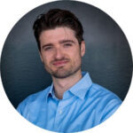
Speaker: Keifer Vermeulen, Head of Research, Delft Circuits
Kiefer Vermeulen works as Head of Research at Delft Circuits. With a background in quantum computing and expertise in flexible circuits for high frequency signals, he has been working for the quantum hardware company almost seven years. In his spare time, he can be found in the boulder hall, practicing Jiu Jitsu, sculpting or making stain-glass art.
Wincal- The Engineer’s Flexible RF Calibration Friend
Available for on demand viewing
WinCal is widely recognized in the industry for its robust RF calibration capabilities. However, it also offers a range of lesser-known features that make it an integral part of an analytics pipeline or a cost-effective, feature-rich test executive.
This webinar will showcase these advanced analysis features and demonstrate how WinCal can be seamlessly integrated with popular open-source software packages. By leveraging WinCal's powerful algorithms, users can significantly enhance its functionality. The latest 5.1 release introduces several new APIs designed to facilitate this integration, which will be discussed in detail.

Gavin Fisher, Senior Staff Applications Specialist, FormFactor Inc.
Gavin Fisher is a member of the Centre of Expertise group at FormFactor, providing application support and technical services to FormFactor’s customers. With more than 2 decades of experience working with Cascade probe systems, and with his deep technical knowledge in a broad spectrum of applications such as high-frequency measurement, measurement automation, calibration and power device measurement, he educates and trains customers on best practices to achieve accurate measurement results. He has made several presentations at European Microwave Week, MOS-AK workshops, and Agilent/Keysight seminars.
Prior to joining FormFactor, Gavin served as a Mechanical Engineer at Alenia Marconi Systems. He holds an upper-second degree from Brunel University in Mechanical Engineering with electronic systems.

James Hibbert, Principal Applications Engineer, FormFactor Inc.
James is a key member of FormFactor's Centre of Expertise, a group comprised of highly experienced engineers and technical specialists responsible for advancing the frontiers of semiconductor wafer testing and measurement. He is specifically focused on overcoming the challenges of accurately characterising RF devices, particularly for emerging applications such as 6G.
Prior to his tenure at FormFactor, James was an electronics engineer at Fotenix and interned at Broadcom.
He received a doctorate in Electrical Engineering from University of Manchester.
Autonomous RF Measurements: Hands-Free Recalibration and Drift Compensation Across Multiple Temperatures
Available for on demand viewing
The Autonomous RF measurement assistant combines programmable positioners, a precise digital microscopy system, and advanced pattern recognition algorithms to enable fully autonomous, hands-free calibrations and measurements of RF devices over multiple temperatures.
This system manages the entire test flow for thermal and ambient testing, including automated calibration, monitoring to prevent measurement drift, and adjustment of probe spacing to account for growth and different probing geometries.
This presentation demonstrates the use of this approach for MLTRL calibrations both off and on wafer, showcasing the interaction between WinCal, Python, and analytical methods to evaluate calibration repeatability. Additionally, We will discuss the probe placement for unattended long-duration RF measurements.

Pranav Shrivastava, Principal Applications Engineer
Pranav K. Shrivastava works as an application engineer in FormFactor GmbH Germany as a team member of CoE team at FFI. His area of specialization is RF and Microwave Engineering, and mostly working for the solutions towards automated high frequency on-wafer measurements. His main research interests during his Ph.D. work involved RF micromachined components in mmWave range, phases shifters, RF MEMS switch, Sub-THz range metastructure and their characterization.
Velox Dash™ - A Modern Touchscreen-Based Interface for Intuitive Probe Station Control
Available for on demand viewing
FormFactor's new companion device is here! Velox Dash™ enhances probe station control by providing access to the most used functionalities with just a touch of a finger. With its modern user interface, Velox Dash sets a standard for easy-to-use operation of engineering probe stations. The companion device combines an intuitive touch interface with an adaptable workplace.
Additionally, Velox Dash consolidates the functionalities of hardware joystick and eVue remote control into a single platform. The novel Velox Dash's user-centered design makes daily work a gratifying experience.
Attend this webinar and learn the latest features and functionality.

Dr. Velimir Meded, Sr Principal Applications Engineer
Dr Velimir Meded, is a physicist with a focus on multidisciplinary integration and systemic solutions as well as with more than 40 scientific publications under his belt. Dr Meded works as an applications engineer in Centre of Expertise, Systems BU located in Dresden, Germany. While his work focuses on cryogenic and high power systems, he is also very active in general integration problems including artificial intelligence. As a member of the Velox Dash project core team, he is uniquely positioned to tell us more about both the features and the development roadmap of Velox Dash.
Inclined vs. Horizontal Waveguide Port Saver Approach in WR3.4 Band for On-Wafer Measurements
Available for on demand viewing
High frequency on-wafer measurements require waveguide based frequency extenders. As a company, FormFactor make extensive use of inclined frequency extenders, both coaxial single sweep and also banded Waveguide. The approach is very convenient for wafer probers where the platen is thermally optimized with insulation layers, to get the very best positioning stability for the probes and positioning mechanics.
One key benefit of this approach is by their very nature, the extenders are further away from the hot wafer chuck which inherently should improve temperature stability. However up until this point our evaluation of these approaches was limited to 220 GHz and ambient conditions only. In the work we contrast and compare the stability of the inclined approach versus direct connected horizontal, both for the ambient and over temperature cases. T-wave probes and waveguide-based infinity probes are used for observations in WR3.4 band.
Risk Mitigation Strategies for mmWave Production Test Environments
Available for on demand viewing
With the 5G mobile network in full deployment, antenna transceivers operating in the 24.25 GHz to 43.5 GHz frequency bands have become integral components of high-end smartphones. These transceivers utilize advanced beam steering and beamforming techniques to optimize wireless data transmission, necessitating precise phase control across up to 32 RF signals. Ensuring these chips are verified as Known Good Die prior to module integration is crucial, demanding probe cards and testing equipment that deliver laboratory-grade precision in RF measurements at production scales.
Employing membrane-based probe technologies meets the electrical demands which results in higher forces, necessitating meticulous setup and system deflection management to ensure optimal contact performance and durability. This challenge is further compounded when scaling test parallelism to reduce the Cost of Test. For instance, with an eight-site probe head configuration, there are hundreds of nets, nearly a third of them being RF signals, interacting through approximately 5000 probe contacts, and resulting 50-80 kg of probing force.
This presentation delves into several strategies and the utilization of specific equipment to gather empirical data on Actual vs. Programmed Overtravel in multi-site RF probe cards. We will explore how this data informs the development of baseline models for predictive Finite Element Analysis modeling, paving the way for enhancements in future applications. These methodologies mitigate some of the prevalent risks associated with mmWave chip testing in high-volume manufacturing contexts, ultimately contributing to a reduction in the overall Cost of Test.

Kevin Ayers, Senior Staff Mechanical Engineer
Kevin Ayers is a senior mechanical design engineer with 24 years of design experience specializing in electronic equipment and semiconductor test. At FormFactor he is responsible for developing and productizing new probe technologies. Prior to joining FormFactor, Kevin worked at Tektronix architecting, planning, and designing next generation oscilloscopes. He holds a degree in mechanical engineering from University of Washington.
.

Ryan Garrison, Senior Product Manager
Ryan Garrison is a Senior Product Business Manager with FormFactor’s Probes BU focused on RF probing solutions. With over 20 years at FormFactor, he has held multiple engineering and leadership roles in operations and the development of Analytical RF Probes, Probe Stations, and now Production RF Probes. His current responsibility centers on the business of expanding RF test parallelism for sub-6 GHz and mmW antenna devices. Most recently Ryan lead a team through the development-process-to-product-release of a new probe head effectively doubling the parallelism of RF test using FormFactor’s membrane technology. Prior to joining FormFactor, Ryan graduated from the Oregon State University in Industrial and Manufacturing Engineering.
Making Accurate and Consistent Wafer Measurements with Next Generation Guarded True-Kelvin MEMS DC Probes
Available for on demand viewing
Gate length down-scaling of silicon-based transistor results in very small on-state drain-source resistance, making it challenging for test engineers to perform precise and repeatable wafer measurements. Size reduction of aluminum-capped copper test pads to save on lithography, prototyping and production costs implies that it is very difficult to re-probe the same device with low contact resistance. Novel true-Kelvin MEMS analytical DC probes, new test and modelling strategies are proposed in this work to address these emerging test challenges.

Dr. Choon Beng Sia, Technical Director, Applications Engineering
Dr Choon Beng Sia is a SSG Fellow, conferred by the President of the Republic of Singapore. At FormFactor’s Center of Expertise, he is a Technical Director responsible for developing solutions to overcome semiconductor wafer test challenges. Dr Sia serves in the IEEE MTT-3 technical committee, defining standards and best practices for RF measurements. He is also a lecturer of the MTT-3 speaker bureau, specialising in wafer RF and 5G tests. Dr Sia is a recipient of multiple best paper awards at international conferences, publishing more than 50 scientific papers, holding 13 international patents.
使用下一代Guarded, True Kelvin MEMS 直流探针進行準確、一致的晶圓測量
Available for on demand viewing
Gate length down-scaling of silicon-based transistor results in very small on-state drain-source resistance, making it challenging for test engineers to perform precise and repeatable wafer measurements. Size reduction of aluminum-capped copper test pads to save on lithography, prototyping and production costs implies that it is very difficult to re-probe the same device with low contact resistance. Novel true-Kelvin MEMS analytical DC probes, new test and modelling strategies are proposed in this work to address these emerging test challenges.

Dr. Choon Beng Sia, Technical Director, Applications Engineering
Dr Choon Beng Sia is a SSG Fellow, conferred by the President of the Republic of Singapore. At FormFactor’s Center of Expertise, he is a Technical Director responsible for developing solutions to overcome semiconductor wafer test challenges. Dr Sia serves in the IEEE MTT-3 technical committee, defining standards and best practices for RF measurements. He is also a lecturer of the MTT-3 speaker bureau, specialising in wafer RF and 5G tests. Dr Sia is a recipient of multiple best paper awards at international conferences, publishing more than 50 scientific papers, holding 13 international patents.
How to Build a Quantum Computer- A FormFactor & Tabor Electronics Collaboration
Available for on demand viewing
Quantum computing is reaching an inflection point. Once a technology developed and operated in experimental labs, is now being manufactured by large-scale industrial companies. The commercialization of superconducting quantum processing units (QPUs), FPGA-based microwave synthesis electronics, and ultra-low-temperature refrigerators, has resulted in the realization of a commercial-off-the-shelf, full-stack quantum systems. Such full-stack systems can be operated with ease by the end-user and enable rapid testing and characterization of qubit systems, significantly reducing the cost and time involved in such measurements and allowing for further advancements in quantum computing technology.
In this webinar we show the results of an industry collaboration between Tabor Electronics and FormFactor, Inc. using the QuantWare 5-qubit QPU. We detail the system architecture and show the results of qubit characterization. The 5-qubit QuantWare Soprano QPU is installed in a LF-600 dilution refrigerator provided by FormFactor, Inc with measurement and control performed using the Tabor Proteus P9484M-AWT PXI platform and Tabor’s Qubit Characterization software.
Moderator - Mark Elo, Chief Marketing Officer, Tabor Electronics Ltd.
Mark Elo joined Tabor Electronics Ltd. in 2019 as the US National Sales Manager for Tabor Electronics. On July 2020 he was named VP and GM for the Americas, in April 2022 he became Tabor's CMO (Chief Marketing Officer).
Mark has over 30 years of cross functional test and measurement experience in instrumentation. Mark began his career as a design engineer in Hewlett-Packard's Microwave Division and has since held various senior positions at Agilent Technologies, Anritsu, Gigatronics Tektronix and Keithley Instruments in R&D, sales, marketing and business development.
He has an Honors degree in Solid State Electronics and an MBA.

Speaker - Joe Yeager, Quantum Application Specialist, FormFactor Inc.
Joe Yeager has worked as a quantum and cryogenics application specialist at FormFactor for 2 years. He uses his 20 years of experience in cryogenics and low temperature physics to provide expert support for the company's cryogenic test and measurement solutions. He holds a PhD from Kent State University and worked as a postdoc at NASA Goddard Space Flight Center. Along with his deep technical knowledge, Joe’s experience extends to account and product management with sales and marketing roles at Lakeshore Cryotronics, Oxford Instruments, and Agilent Technologies.

Speaker - Xiaoyue Jin, Chief Quantum Scientist, Tabor Electronics
Xiaoyue Jin is a skilled experimental physicist with expertise in quantum control and operations, particularly in the development and optimization of two-qubit gates between superconducting qubits. He holds a Master of Science degree from Peking University and a Dr. rer. nat. degree from Erlangen University, Germany, graduating with summa cum laude. He later moved to the US and worked as a postdoctoral associate at Massachusetts Institute of Technology. Jin joined National Institute of Standards and Technology (NIST) Boulder, Colorado in 2015, and works first as a Physicist, and later as a Guest Researcher until now. Jin currently also serves as the Chief Quantum Scientist at Tabor Electronics, an Israel-based electronics company focusing on FPGA-based DDS systems as a quantum solution.
Quantum and CryoCMOS: Enabling the Future of Computing with Advanced Test & Measurement Tools
Available for on demand viewing
Advanced computing and quantum computing devices require cryogenic conditions for the processor itself as well as the control chips that drive microwave signal to the processor. These advanced devices typically include niobium or aluminum superconducting circuits, and their support chips are based on cryogenic compatible CMOS structures. Bringing this new technology from the research and development phase, out of the lab and into engineering scale production and ultimately volume production requires specialized tools to test, measure, and deploy the advanced devices all in sub-4K environments. The major bottlenecks include time-consuming wire bonding, expensive packaging processes prior to device cooldown, and long cooldown times for dilution refrigerators.
FormFactor is the leading enabler of quantum computing developers with its suite of cryogenic test and measurement tools as well as deployment solutions. We discuss a customer case study implementing cryogenic wafer probing on SFQ circuits to obtain statistical datasets in hours that would otherwise take weeks or months, a new tool for rapid die testing that makes use of a cryogenic high-density MEMS probe head, enabling photonics probing below 2K, and the deployment of quantum devices in milli-Kelvin dilution refrigerator cryostats with a probe socket interface.
About the host:
Jack DeGrave, Director of Business Development, FormFactor Inc.
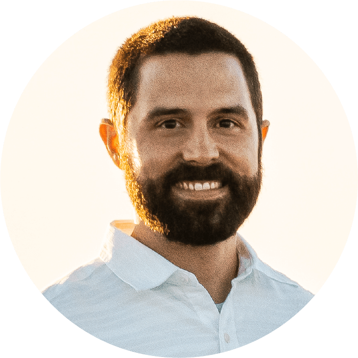
Jack DeGrave joined the FormFactor-HPD Business Development team in early 2021 where he has focused on engaging with the Quantum Development Community members to map out the needs for cryogenic test and measurement, high density I/O device interfacing, and cryostats for deployment of quantum processors. His background in cryogenic test and measurement dates to early 2010 during his PhD studies in low temperature transport properties of helimagnets and skyrmions at the University of Wisconsin-Madison. After graduating, he held business development positions at several cryogenics companies. Jack brings greater than a decade of experience in cryogenic system design and test & measurement.
COMPASS 2023 - Video Presentations Available
Available for on demand viewing @ compass.formfactor.com
The 2023 COMPASS Theme is Megatrends in Test and Measurement
FormFactor’s COMPASS test and measurement community event brings together FormFactor customers from around the world to discuss the products and technologies shaping our future. Industry leaders and speakers from corporations, leading-edge research institutions and FormFactor share test insights on a wide variety of emerging applications including 5G, trends in advanced packages, next generation memories and other devices, ultra-low noise testing, cryogenic probing and millimeter-wave measurement and calibration.
Presentations include:
- Welcome & Executive Address
- Keynote Presentation - Advanced Packaging: Enabling Moore’s Law’s Next Frontier
- Pyramid Probe: RF Calibration and Probe Aging Considerations in HVM High Speed IO Devices
- How FormFactor’s Known Good Die Test Enables Advanced Packaging for High Bandwidth Memory – Solutions and Latest Trends
- Pharos Vertical and Edge Coupling Low Loss SiPh Wafer Test with Fully Automated Calibration - From Probe Install to Successful V-groove Wafer Level Test in 90 Minutes
- Measuring Superconducting Material Properties for Cryogenic Chip Development
- Maximizing CCC in a Probe Card and the March to an Unburnable Probe
- Achieving Traceable RFCMOS Ft and Fmax Wafer Measurements
- Simplifying Photonic Test & Measurement at Cryogenic Temperatures
- Next Generation DC Probes for Accurate and Repeatable Device Modelling Measurements
Next Generation DC Probes for Accurate and Repeatable Device Modelling Measurements
Available for on demand viewing
The semiconductor industry continues to see the relentless downscaling of gate length and development of new architectures for silicon-based transistor to 2 nm and beyond. The on-state currents of such advanced transistors are increasing with decreasing supply voltages. Their off-state currents are kept very low to reduce power consumption. Smaller test pads to reduce lithography costs and the use of copper backend metallization have increased the difficulties for probes to have low and stable contact resistance as there are little fresh pad metal available for deeper probe scrubs or re-probing. These issues aggravate especially at elevated temperatures when the pad aluminum cap layers have been probed and their underlying copper metallization oxidize rapidly, hindering the ability to achieve good probe contacts. In this talk, we introduce the next generation advanced guarded DC probes with small probe scrubs, low leakage performance and true Kelvin force sense probe tips to address the test challenges of making precise and consistent device modelling wafer measurements.
About the host:
Connor Smith, Principal Applications Engineer, FormFactor Inc.
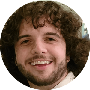
Connor is an application engineer with FormFactor working out of our Boulder CO cryogenic lab. His main function is to help customers to solve their testing problem through configuration of products or test services. While Connor started in the cryogenic lab at FormFactor, he currently supports the probe systems business unit.
Prior to working at FormFactor, Connor was active during his years as a student at Colorado School of Mines where he worked as a lab assistant and community director while studying mechanical engineering.
Making Traceable and Accurate sub-THz Measurements for Wafer Test Applications.
Available for on demand viewing
To support the development of 6G and beyond mobile communication products, wafer S-parameters and RF measurements at sub-THz frequencies are becoming common, daily measurements for test engineers. Accuracy, repeatability and traceability in tests, particularly for active devices, are necessary requirements as test engineers collaborate among their colleagues and customers in labs of various geographical locations. In this talk, based on published IEEE papers, we are going to discuss how probe tip power calibration, continuity checks in banded sub-THz measurements, probe tip contact resistance monitoring as well as best practices in autonomous over-temperature high frequency measurements, can help to address these evolving test requirements.
About the host:
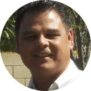
Jason Alikpala, Sr. Staff Applications Engineer, FormFactor
Jason is a senior applications engineer with over a decade of experience in RF and DC probes, probe control software and on-wafer calibration at FormFactor. He is an expert in modeling and characterization having led strategic planning and implementation of product releases while serving as R&D manager for Agilent and Hewlett Packard.
He holds a BS in electrical engineering from Cal State Polytechnic University at Pomona.
Considerations for Vertical High Probe Count Testing
Available for on demand viewing
As semiconductor suppliers strive to increase their throughput and lower their test costs, probe card parallelism continues to increase. State of the art probe card designs require up to 80,000 probes and the industry is driving for as much as 150,000 probes in the future. Where are the limitations? Total probe force will be >200 kgf and while there are testers that can handle this amount of force, probe card deflection needs to be considered to maintain high volume production requirements.
Today, the ratio of actual overtravel on the probes to the programmed overtravel can be as low as 30% which makes achieving low contact resistance between probe tip and wafer a challenge. Increasing probe card stiffness is simple in theory but the space constraints between probe card and tester plus the need to populate the PCB with many components makes this very difficult to achieve. In addition to the tester, the prober and probe card metrology tools will need to accommodate this higher force as well.
This webinar will provide a survey of the test equipment industry and identify the chief limitations including where probe card mechanical design needs to improve.
About the host:
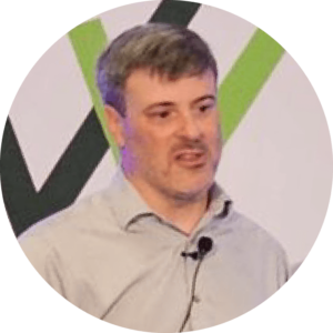
Keith Martin, Sr. Director Product Marketing, FormFactor Inc.
Keith is an accomplished leader in the semiconductor industry with more than 19 years experience working for capital equipment and semiconductor logic device manufacturers including Intel and Lam Research. He has applied his expertise in process development, mechanical engineering, and materials science to develop manufacturing equipment and processes in the areas of probe card manufacturing, thin film deposition, and photolithography. His experience also extends to factory start-ups of 300mm fabs as well as probe card manufacturing facilities.
Keith holds a BS in Mechanical Engineering from Johns Hopkins University and a Ph.D. in Materials Science from Northwestern University.
Scaling Measurement Methodologies Using Cryogenic TaaS Framework for Higher Quality cryo-LNAs and Reliable Qubit Readout Chains
Available for on demand viewing
As superconducting quantum computers scale, cryogenic microwave components in the qubit control and readout chain must be appropriately tested and qualified to ensure the consistency and high fidelity of quantum computation. Furthermore, system uptime is critical for commercialization, which is dependent on reliably predicting maintenance cycles and expediting downtime recovery. Both requirements highlight the need for standardized measurement protocols to scale the test capability in the industry. Here we will examine a test framework where we describe procedures for conducting functional, reliability, and integrated testing on cryogenic components. Our pilot use-case investigates calibration and test methodologies for gain and noise figure measurements of low temperature LNAs. Finally, we will discuss how to scale these measurements for high volume reliability testing.
About the host:
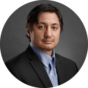
Brandon Boiko, Sr. Applications Engineer, FormFactor Inc.
Brandon is a senior applications engineer with FormFactor Inc. as part of the cryogenics HPD product group. He attended the University of Colorado in Boulder where he earned both his bachelor’s and master’s degree in mechanical engineering. Starting his cryogenics career in 2015 at High Precision Devices, Brandon has more than 8 years of experience designing low temperature equipment. In Fall of 2021 FormFactor initiated the Advanced Cryogenics Lab where he is currently leading the development of cryogenic test as a service.
New: Entry-Level Silicon Photonics Solution for Fundamental Research
Available for on demand viewing
FormFactor introduces a cost-effective silicon photonics measurement solution to support fundamental research work for emerging applications.
Designed into the system are FormFactor's years of experience developing automated photonics measurement systems – now tailored to the needs of universities and other entry-level users. Leveraging its intuitive design, the MPS150-SiPh is the perfect solution for less experienced users to discover photonics and achieve highest accuracy test results.
- Supports both surface coupling and horizontal edge coupling
- Aligns optical fibers to couple light in and out of a device without physical contact
Learn how this new solution can help entry-level photonics researchers achieve:
- Optimal measurement performance by precise placement of optical fibers
- Better precision through theta angle adjustment of optical probes
- Faster measurement results with optional, automated positioners
- Coverage of multiple probing applications by converting the platform for use in RF, IV/CV or failure analysis in just a few steps
About the host:

Tino Minner, Sr. Manager Strategic Marketing, FormFactor Inc.
As a graduate engineer specializing in mechanical engineering and business administration, Tino can look back on many years of professional experience in semiconductors. He started his career at FormFactor in 2015 in the product management department, followed by the management of the used equipment and strategic marketing division from where he then took over the Silicon Photonics market segment.
FRT MicroProf® PT – A New Metrology and Inspection Solutions for Advanced Packaging
Available for on demand viewing
Fan-out panel level packaging is currently one of the latest assembly and packaging trends in the system-in-package world, meeting the increasing demands for extreme miniaturization and rising system requirements at reduced production costs.
This webinar will introduce a NEW solution- the FRT MicroProf® PT, a semiconductor metrology and inspection tool for rectangular panels up to 600 mm — containing 4-5X more dies compared to a 300 mm wafer and equipped with SurfaceSens™ technology. We'll discuss these important features:
- Metrology and defect inspection applications in one tool
- Full automation with two loaders for panel FOUPs, for panels up to 600mm x 600mm in a SEMI-compliant EFEM
- Multi-sensor setup including topography, field-of-view and film thickness with hybrid software evaluation to evaluate highly complex structures
- Film thickness measurements from micron-range down to tens of nanometers
- Wide range of handling capability – from substrates a few millimeters thick to 200µm, including organic and glass
FRT Metrology specializes in fully automated multi-sensor metrology system for application-specific advanced packaging (ASAP) measurements from development to production (lab to fab). We will also cover interesting challenges this new technology means for metrology and inspection such as measuring via-like structures in patterned photoresist and handling large panels instead of wafers.
About the host:
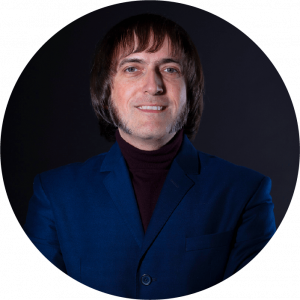
Bastian Tröger, Team leader of Product Management and Field Application, FormFactor Inc.
As a graduate engineer specializing in physical optics, Bastian can look back on many years of professional experience in optical metrology. His career at FRT started in 2007 in the development department, followed by the establishment of a new product management department and eventually led him to the management level of FormFactor FRT Metrology.
WinCal 5 Software: Improved Functionality and Features for Better Test Outcomes
Available for on demand viewing
For more than 30 years, WinCal has been the market-leading RF calibration software. In recent years, improvements in usability and features have made the software the best-in-class for RF test and measurement. The latest version of WinCal 5.0 builds upon these improvements and offers even more functionalities.
Attend this webinar and learn:
- An overview of the new modernized WinCal 5.0 user interface
- New 1-port Least Square Calibration algorithm
- Strategies to leverage the software's vast capabilities for measurements and post-processing
We will discuss the new user interface approaches to streamline fast and efficient system configuration and operation. This includes increased homogenization with our market-leading Velox™ probe station control software. We will show the groundbreaking work space approach to dynamically optimize the measurement environment and suit device and measurement needs.
About the host:

Gavin Fisher | Senior Applications Engineer at FormFactor Inc.
Gavin Fisher is a member of the Centre of Expertise group at FormFactor, providing application support and technical services to FormFactor’s customers. With more than 2 decades of experience working with Cascade probe systems, and with his deep technical knowledge in a broad spectrum of applications such as high-frequency measurement, measurement automation, calibration and power device measurement, he educates and trains customers on best practices to achieve accurate measurement results. He has made several presentations at European Microwave Week, MOS-AK workshops, and Agilent/Keysight seminars.
Prior to joining FormFactor, Gavin served as a Mechanical Engineer at Alenia Marconi Systems. He holds an upper-second degree from Brunel University in Mechanical Engineering with electronic systems.
Advances in Analytical Wafer Probing of High-voltage / High-current Devices
Available for on demand viewing
With electric vehicles and other high-power applications gaining momentum, the development of new high-voltage/high current semiconductor devices is ramping up. Wafer test of these power semiconductors poses unique challenges, with test currents of more than 500 Amps and test voltages up to 10 Kilovolts. Designers of these new devices are pushing the limits of physics by shrinking the distance between contacts and requiring test temperatures up to 200° C. In addition, new materials such as silicon carbide and gallium nitride are growing in popularity, adding new complexity to carry out testing in an environment that suppresses electrical arcing, provides low contact resistance of the probe to the device, and low contact and thermal resistance with uniformity between the wafer and chuck. Analytical and engineering probing is key in the research and development of these leading edge semiconductor technologies.
In this webinar, Rainer Gaggl, Founder and Managing Director of T.I.P.S. Messtechnik GmbH (specialists in the design and manufacturing of high-power wafer probe cards), and FormFactor’s Eric Wilcox, Director of Product Marketing, discuss these wafer test challenges and patented high voltage arc suppression technology that provides spark-free probing for high-voltage / high-current devices made with Si, SiC and GaN technology.
About the hosts:
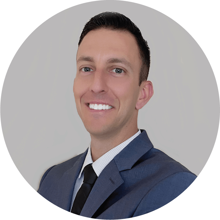
Eric Wilcox, Director, Marketing, DC and High-Power Market Segments, FormFactor, Inc.
Eric Wilcox is the Director of Marketing for FormFactor’s DC and High-Power Market Segments. Mr. Wilcox has held multiple organizational roles within the company, including Senior Marketing Manager for the Probe Systems business and Product Marketing Manager for the Reliability Test Systems business. Prior to this, Mr. Wilcox was a Senior Applications Engineer in the Center of Expertise at Cascade Microtech, Inc., and was responsible for the worldwide technical leadership of Reliability Test Products. Mr. Wilcox has co-authored multiple papers with industry experts about next generation reliability test methodologies for presentation at some of the premier IEEE reliability conferences and has obtained a US patent for innovative systems and methods of performing electromigration testing. Mr. Wilcox holds a Bachelor of Science in Business Management from the University of Northwestern – St. Paul.
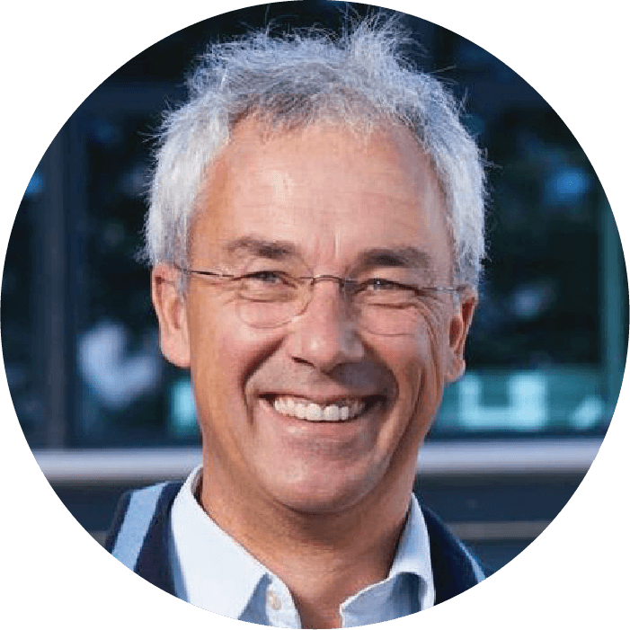
Rainer Gaggl, Founder and Managing Director, T.I.P.S. Messtechnik GmbH
Rainer Gaggl is managing director of T.I.P.S. Messtechnik GmbH and responsible for product and process development as well as strategic sales activities. Mr. Gaggl founded T.I.P.S. in 1997 as a "spin-off" of Siemens Bauelemente; the company today has grown to a more than 80-person workforce headquartered in Villach, Austria. The main focus of his work is on test interfaces for high power devices, automotive ASICS, sensors and MEMS devices, and automotive RADAR. High voltage, high currents and probe cards with sensor stimuli are some of his "playgrounds as a physicist" and he holds several patents in that field. He holds a Ph.D. in Physics from the Technical University of Graz.
A Beginner's Guide to Quantum Computing
Available for on demand viewing
| Quantum computing promises to revolutionize the way we address complex issues and deliver world-changing solutions in medicine, security, finance, defense, climate, energy, and more. Around the globe, governments, universities, and industry players of all sizes are investing tens of billions of dollars in the race to transform this amazing potential from theory into reality in the next few years.
In this webinar, authors Dr. Hiu Yung Wong and Dr. Zuyu Zhao will share their expertise in quantum computing. Attendees will learn:
Twenty webinar attendees will be randomly chosen to receive one of their works, “Introduction to Quantum Computing, From a Layperson to a Programmer in 30 Steps,” (Dr. Hiu Yung Wong) or “Cryogenic Engineering and Technologies, Principles and Applications of Cryogen-Free Systems,” (Dr. Zuyu Zhao / Dr. Chao Wang). Register today! |
About the hosts:

Dr. Zuyu Zhao, Chief Cryogenic Scientist, FormFactor, Inc.
Dr. Zuyu Zhao is Chief Cryogenic Scientist at FormFactor, having joined the company in June 2022 through the acquisition of JanisULT. Dr. Zhao has more than 25 years in the cryogenic field, with specialization in Dilution Refrigerators. Dr. Zhao joined Janis Research Company in 1993 and focused on developing custom ultra-low temperature facilities for the research and science community. He then served on the Board of Directors and as Vice President-Principal Scientist of the company. He also served from July 1, 2007 through June 30, 2013 as an elected member of the American Institute of Physics (Physics Today) Advisory Committee. Dr. Zhao received his B.S. degree from Fudan University in 1982, Class 77. He came to the United States in 1983 with the World Bank Scholarship program and graduated from Northwestern University with a Ph.D. degree of physics in 1990. He then spent two and a half years working at Harvard University as a post-doc and set up a new lab pursuing Bose-Einstein condensation on spin polarized hydrogen.

Dr. Hiu Yung Wong, Assistant Professor and Silicon Valley AMDT Endowed Chair in Electrical Engineering, San Jose State University
Dr. Hiu Yung Wong is an Assistant Professor and Silicon Valley AMDT Endowed Chair in Electrical Engineering, San Jose State University. He received his Ph.D. degree in EECS from UC Berkeley in 2006. From 2006 to 2009, he worked as a Technology Integration Engineer in Spansion. From 2009 to 2018, he was a TCAD Senior Staff Application Engineer in Synopsys. He received the Curtis W. McGraw Research Award from ASEE Engineering Research Council in 2022, the NSF CAREER award and the Newnan Brothers Award for Faculty Excellence in 2021, and Synopsys Excellence Award in 2010. He is the author of the book, "Introduction to Quantum Computing: From a Layperson to a Programmer in 30 Steps". His research interests include the applications of machine learning in simulation and manufacturing, quantum computing, cryogenic electronics, reliability simulations, wide bandgap device simulations, and Design Technology Co-Optimization (DTCO). His works have produced one book, along with a book chapter, 90 papers, and 10 issued patents.
Best Approaches for Sub THz Over Temperature Wafer Test
Available for on demand viewing
Wafer probing has been done for some time in waveguide at frequencies up to several hundreds of GHz. However solutions were typically limited by the constraints of large format extenders with large format positioners, which could limit the capabilities for over temperature work or RF performance.
Recent advances from Virginia Diodes Inc. and Formfactor, have allowed for solutions that allow optimal path lengths and the ability to isolate the extenders from elevated thermal temperatures while still also carrying out cold / dry / dark measurements.
In the talk we will discuss:
- Latest solutions for optimal path length and over temperature capability
- Best practices to optimise calibration and system drift
- Use of Wincal as a tool to evaluate system performance
- Autonomous RF to allow for fully automated calibration including Multiline TRL as well as automated device measurements over temperature at Sub THz frequencies
- Real life measurement results
About the hosts:

Gavin Fisher | Senior Applications Engineer at FormFactor Inc.
Gavin Fisher is a member of the Centre of Expertise group at FormFactor, providing application support and technical services to FormFactor’s customers. With more than 2 decades of experience working with Cascade probe systems, and with his deep technical knowledge in a broad spectrum of applications such as high-frequency measurement, measurement automation, calibration and power device measurement, he educates and trains customers on best practices to achieve accurate measurement results. He has made several presentations at European Microwave Week, MOS-AK workshops, and Agilent/Keysight seminars.
Prior to joining FormFactor, Gavin served as a Mechanical Engineer at Alenia Marconi Systems. He holds an upper-second degree from Brunel University in Mechanical Engineering with electronic systems.

Jeffrey Hesler, CTO & Owner, Virginia Diodes, Inc.
Jeffrey L Hesler is the CTO of Virginia Diodes and a visiting faculty at the University of Virginia. For more than 25 years he has worked to create new technologies that utilize the Terahertz (THz) frequency band for scientific, defense, and industrial applications. He has published over 200 technical papers, is a member of IEEE Technical Committee MTT-21 (THz Technology and Applications) and is a co-Editor of the IEEE Transactions on Terahertz Science and Technology. Terahertz systems based on his innovative designs are now used in hundreds of research laboratories throughout the world.
Delivering Advanced mm-Wave Load-Pull Measurements
Available for on demand viewing
The ramp-up of 5G mm-Wave technologies comes with substantial enhancements in connectivity, promising to revolutionize our world. A fundamental requirement of 5G devices is to maximize performance by optimizing the power and/or effciency of the amplifiers and transistors. This is done by measuring the performance characteristics of the device at different impedances that are systematically changed using load-pull tuners.
FormFactor has partnered with Focus Microwaves and Keysight Technologies to deliver a fully integrated probe solution for accurate on-wafer mm-Wave load-pull measurements, delivering a number of benefits along the way, including:
- Low-Loss Measurement Channel for Maximized Tuning Range
- Accurate Probing of Small Pads for High Resolution with a Perfect Fit
- Coaxial Calibration with the Highest Phase Stability
- EMI and light-tight testing at a wide temperature range, including tests down to -40°C without a build-up of frost and condensation.
About the hosts:
Anthony Lord | Director, RF Segment Business Development at FormFactor Inc.
Anthony Lord is Director, RF Segment Business Development for FormFactor’s Systems Business Unit. Anthony has been involved in many organizational roles within the company, including applications engineering, sales management, product line management, strategic marketing as well as segment marketing, and has been actively involved in the semiconductor and RF industry for 24 years. Anthony has published several papers on RF on-wafer measurements, and has hosted numerous workshops and presentations on on-wafer test applications. Currently, Anthony is exploring where the RF semiconductor market is heading, and how to position future products to enable engineers to make the most accurate measurements with the fastest time to data.
Vince Mallette | Executive Vice President at Focus Microwaves
Vince Mallette receieved his B.Sc from the University of Quebec - ETS in Montreal, Quebec, Canada in 2004. He has over 15 years of industry experience with Agilent (now Keysight), Focus Microwaves group pursuing product innovation, development and strategic business development. Currently he is the Executive Vice President of Focus Microwaves and heads all major business initiatives in terms of partnerships and growth on technology evaluation front. He has supported all different foundries ranging from silicon to III-V technologies from sub 6 GHz to mm-wave frequencies and innovation in tuner space from single frequency to harmonic tuner enabling high performance out of the device. He has authored and coauthored over 10 referred publications.
FRT Metrology for Advanced Packaging - Ensuring the highest quality control of grinding and dicing processes for DISCO Hi-Tec Europe
Available for on demand viewing
Advanced packages have enabled the industry to develop new flip-chip processes, 2.5D interposer and TSV technology, and 2D and 3D fan-out processes with high densities of connections in the smallest of spaces. With these new innovations, the need for flexibility in wafer metrology and handling has exploded. FormFactor MicroProf® AP metrology tools are specifically designed to address an extensive list of advanced packaging format and application challenges.
DISCO Hi-Tec Europe, a technological leader in grinding and dicing processes, will discuss how they perform advanced metrology using FormFactor FRT MicroProf® AP multi-sensor tools equipped with SurfaceSensTM technology to ensure the highest quality control of these processes.
Join us for this webinar to learn about:
- Metrology applications in advanced packaging
- Best practices and tips for grinding and dicing processes
- How the FRT MicroProf® helps support the highest quality control of processes
About the hosts:
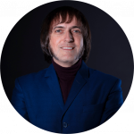
Bastian Tröger | Team leader of Product Management and Field Application, FormFactor FRT Metrology
Team leader of Product Management and Field Application, FormFactor FRT Metrology
As a graduate engineer specializing in physical optics, he can look back on many years of professional experience in optical metrology.
His career at FRT started in 2007 in the development department, followed by the establishment of a new product management department and eventually led him to the management level of FormFactor FRT Metrology.

Dietmar Mayer | Manager of Dicing-Grinding Service, Disco Hi-Tec Europe GmbH
Manager of Dicing-Grinding Service, Disco Hi-Tec Europe GmbH
Dietmar started his career 1997 as a technician in the semiconductor field before he joined Disco Hi-Tec Europe GmbH in 2005.
He established an unique service solution in Dicing/Grinding/Polishing for semiconductor production worldwide as a supply chain partner for application support/improvement, prototype development or mass production.
New Solutions for Analytical Wafer Probing of Silicon and Wide Band Gap Power Devices
Available for on demand viewing
The increasing use of electric vehicles, renewable energy sources, and other high-power industrial applications continues to drive the development of new high-voltage/high current semiconductor devices. While wide band gap (WBG) based devices have many advantages in high power circuits, time to market constraints often dictate the need to test these types of advanced devices on-wafer.
Wafer test of these power semiconductors poses unique challenges, as they often require test currents of more than 500 Amps, test voltages up to 10 Kilovolts and test temperatures up to 200° C. In addition, the wafer probing environment creates additional concerns such as the potential for electrical arcing, the need to minimize probe contact resistance to the DUT, and the requirement to maintain low contact and thermal resistance between the wafer and chuck.
This webinar will cover the basics of on-wafer power semiconductor device test, review the challenges listed above, and explain the solutions available to meet these challenges. After listening to this webinar attendees will have a much better understanding of the issues involved with testing advanced power devices on-wafer.
About the hosts:
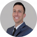
Eric Wilcox, Director, Marketing, DC and High-Power Market Segments, FormFactor, Inc.
Eric Wilcox is the Director of Marketing for FormFactor’s DC and High-Power Market Segments. Mr. Wilcox has held multiple organizational roles within the company, including Senior Marketing Manager for the Probe Systems business and Product Marketing Manager for the Reliability Test Systems business. Prior to this, Mr. Wilcox was a Senior Applications Engineer in the Center of Expertise at Cascade Microtech, Inc., and was responsible for the worldwide technical leadership of Reliability Test Products. Mr. Wilcox has co-authored multiple papers with industry experts about next generation reliability test methodologies for presentation at some of the premier IEEE reliability conferences and has obtained a US patent for innovative systems and methods of performing electromigration testing. Mr. Wilcox holds a Bachelor of Science in Business Management from the University of Northwestern – St. Paul.

Alan Wadsworth, Business Development Manager at Keysight Technologies
Alan Wadsworth is the Americas region Business Development Manager for Precision and Power Products at Keysight Technologies. He has over 30 years of industry experience in both semiconductor design and test, and he is the author of both The Parametric Measurement Handbook and The New Power Handbook. Alan has Bachelor and Master of Science degrees in electrical engineering from the Massachusetts Institute of Technology and an MBA from Santa Clara University.
Overcoming Challenges for Wafer-Level Low Frequency Noise Measurements
Available for on demand viewing
The development of next generation semiconductor device technology nodes targeted for communications, memory, imaging and various analog applications requires advanced wafer level low noise test and measurement capabilities. Flicker noise (1/f), random telegraph noise (RTN), and phase noise have been demonstrated to affect device behaviour and final circuit performance. In today's test labs, it is vital that test engineers are able to accurately measure the device or circuit noise characteristics in a quiet wafer test environment. For this talk, we will first look at the different types of low frequency noise, how they are measured and their impact on devices as well as various circuit applications. We will also discuss the requirements of a quiet wafer test environment and the challenges of achieving one. Finally a wafer test solution that allows test engineers to make accurate low frequency noise measurements will be presented at the end of this talk.
About the hosts:
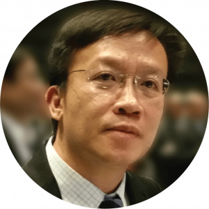
Dr. Sia Choon Beng | Test Technologist at FormFactor Inc.
Dr. Choon Beng Sia is a SSG Fellow, conferred by the President of the Republic of Singapore. He is also a Nanyang Research Scholar and has received doctorate degree in Electronics Engineering from Nanyang Technological University, Singapore with 6 tier-1 journals & 3 conference papers published for his Ph.D. dissertation on RF Design, Characterization and Modelling of Silicon-based Devices.
In his current work at FormFactor as a Test Technologist, Dr Sia develops solutions to overcome semiconductor wafer test and measurement challenges. His research interests include design, test and modelling of silicon-based RF devices, THz calibration and measurements for 5G and IoT applications, photonics and power device wafer tests for LIDAR/Autonomous Transport/Optical communication applications as well as applying data analytics, deep learning and artificial intelligence to wafer tests and device modelling.
Dr. Sia serves in the IEEE MTT-3 technical committee focusing on developing standards and best practices for RF measurements, where he is also a member of the MTT-3 speaker bureau specializing in wafer RF and 5G tests. He lectures graduate-level semiconductor courses for IEEE and Singapore Semiconductor Industry Association. Through SPRING, the National Standards board, Dr. Sia represents Singapore as a Technical Expert in various IEC technical committees, developing standards for MEMs, optical and wafer-level reliability tests for semiconductor devices.
A wafer test, device modelling and process design kit (PDK) expert, Dr. Sia is often consulted by international semiconductor companies, defense, government and medical research institutes. He is a frequent invited speaker and organizer of IEEE workshops, international test forums and presently holds 12 international patents. Dr. Sia has published more than 50 scientific journals and conference publications, of which 85% of them as the first author. His technical papers on 5G production wafer test received multiple "Best Paper" awards and the "Best ATE Paper" award at the 2018, 2019 Semiconductor Wafer Test Conference and 2020 Test Vision Symposium, while his paper on Silicon Photonics wafer test received the "Most Inspirational Paper" award at the 2019 Semiconductor Wafer Test Conference.
克服晶圆级低频噪声测量的挑战
Overcoming Challenges for Wafer-Level Low Frequency Noise Measurements*
Available for on demand viewing
The development of next generation semiconductor device technology nodes targeted for communications, memory, imaging and various analog applications requires advanced wafer level low noise test and measurement capabilities. Flicker noise (1/f), random telegraph noise (RTN), and phase noise have been demonstrated to affect device behaviour and final circuit performance. In today's test labs, it is vital that test engineers are able to accurately measure the device or circuit noise characteristics in a quiet wafer test environment. For this talk, we will first look at the different types of low frequency noise, how they are measured and their impact on devices as well as various circuit applications. We will also discuss the requirements of a quiet wafer test environment and the challenges of achieving one. Finally a wafer test solution that allows test engineers to make accurate low frequency noise measurements will be presented at the end of this talk.
*This webinar will be presented in Chinese language.
About the host:
Dr Sia Choon Beng | Test Technologist at FormFactor Inc.
Dr Choon Beng Sia is a SSG Fellow, conferred by the President of the Republic of Singapore. He is also a Nanyang Research Scholar and has received doctorate degree in Electronics Engineering from Nanyang Technological University, Singapore with 6 tier-1 journals & 3 conference papers published for his Ph.D. dissertation on RF Design, Characterization and Modelling of Silicon-based Devices.
In his current work at FormFactor as a Test Technologist, Dr Sia develops solutions to overcome semiconductor wafer test and measurement challenges. His research interests include design, test and modelling of silicon-based RF devices, THz calibration and measurements for 5G and IoT applications, photonics and power device wafer tests for LIDAR/Autonomous Transport/Optical communication applications as well as applying data analytics, deep learning and artificial intelligence to wafer tests and device modelling.
Dr Sia serves in the IEEE MTT-3 technical committee focusing on developing standards and best practices for RF measurements, where he is also a member of the MTT-3 speaker bureau specialising in wafer RF and 5G tests. He lectures graduate-level semiconductor courses for IEEE and Singapore Semiconductor Industry Association. Through SPRING, the National Standards board, Dr Sia represents Singapore as a Technical Expert in various IEC technical committees, developing standards for MEMs, optical and wafer-level reliability tests for semiconductor devices.
A wafer test, device modelling and process design kit (PDK) expert, Dr Sia is often consulted by international semiconductor companies, defence, government and medical research institutes. He is a frequent invited speaker and organizer of IEEE workshops, international test forums and presently holds 12 international patents. Dr Sia has published more than 50 scientific journals and conference publications, of which 85% of them as the first author. His technical papers on 5G production wafer test received multiple "Best Paper" awards and the "Best ATE Paper" award at the 2018, 2019 Semiconductor Wafer Test Conference and 2020 Test Vision Symposium, while his paper on Silicon Photonics wafer test received the "Most Inspirational Paper" award at the 2019 Semiconductor Wafer Test Conference.
RF Wafer Probing Fundamentals
Available for on demand viewing
An introduction to RF on-wafer probing and calibration. This webinar will expand your knowledge of techniques and tools available to properly characterize RF devices. The webinar is intended for persons interested in RF testing, with beginning knowledge of the physics and characteristics of RF semiconductors.
What you will learn:
- Different RF probe architectures and how to choose the right probe for your application
- On-wafer calibration: S-parameter basics, calibration methods and software
- On-wafer measurement verification
- Design For Testability
- De-embedding
- Temperature testing with RF probes
- Probe cleaning
About the hosts:

Gavin Fisher | Senior Applications Engineer at FormFactor Inc.
Gavin Fisher is a member of the Centre of Expertise group at FormFactor, providing application support and technical services to FormFactor’s customers. With more than 2 decades of experience working with Cascade probe systems, and with his deep technical knowledge in a broad spectrum of applications such as high-frequency measurement, measurement automation, calibration and power device measurement, he educates and trains customers on best practices to achieve accurate measurement results. He has made several presentations at European Microwave Week, MOS-AK workshops, and Agilent/Keysight seminars.
Prior to joining FormFactor, Gavin served as a Mechanical Engineer at Alenia Marconi Systems. He holds an upper-second degree from Brunel University in Mechanical Engineering with electronic systems.
Scanning SQUID Microscopy – Eliminate the guesswork in the design of resilient superconducting circuits
Available for on demand viewing
FormFactor invites you to learn more about scanning SQUID microscopes – their history, applications, and the latest advances for superconducting quantum computing applications. Join IBM Research Division and Stanford University emeritus Dr. John Kirtley, a world-renowned expert who helped develop the technique of scanning SQUID microscopy, and FormFactor’s Dr. Ryan Murdick, Cryogenic Product Development Scientist, who collaborated on developing the industry’s first fully automated, cryogen-free Scanning SQUID Microscope, the IQ1000. By employing SQUIDs capable of magnetometry and susceptometry, the system allows measurements of local magnetization, magnetic response (susceptometry), and the ability to spatially map electrical currents from the magnetic response. Researchers can now rapidly locate and capture detrimental magnetic vortices in superconducting circuits to enable operationally robust IC design and help accelerate the growth of the superconducting quantum computing market.
In this webinar, you will learn:
- What is a scanning SQUID microscope?
- Applications for scanning SQUID technology, and why it’s important for superconducting quantum IC design and characterization.
- The latest advances from FormFactor IQ1000 to enable unattended and high-throughput magnetometry and susceptometry measurements including:
- Automated, fast (five-minute) SQUID tuning
- The ability to measure a large sample (20mm x 20mm) or nine samples (5mm x 5mm) simultaneously in one cool-down
- Superb image quality scanning with sub-100 nm precision, as well as repeatable sub-space scanning and position hold for spectroscopy and vortex manipulation.
- Sample temperature control from <3 K to over 20 K with precise, programmable heating and cooling rates.
About the hosts:

Prof. John Kirtley, Ph.D., consulting professor, Applied Physics Department, Stanford University
John Kirtley has worked in the fields of Surface Enhanced Raman scattering, light emissions from tunnel junctions and electron injection devices, noise in semiconducting devices, scanning tunneling microscopy and scanning SQUID microscopy. Since 2006 he has worked at the University of Twente in the Netherlands, been an Alexander von Humboldt Foundation Forschungspreis winner at the University of Augsburg in Germany, a Jubileum Professor at Chalmers University of Technology in Sweden, and currently holds a Chaire d'Excellence from the NanoSciences Fondation in Grenoble, France.
Kirtley shared the 1998 Oliver E. Buckley Prize with C.C. Tsuei, Donald Ginsberg, and D.J. van Harlingen. The citation was for "using phase-sensitive experiments in the elucidation of the orbital symmetry of the pairing function in high-Tc superconductors". Kirtley, Tsuei, and co-workers used scanning SQUID imaging of the half-integer flux quantum effect in tricrystal samples to demonstrate that cuprate high temperature superconductors have predominantly d-wave pairing symmetry. He received his BA in Physics in 1971 and his PhD in Physics in 1976, both from the University of California, Santa Barbara.
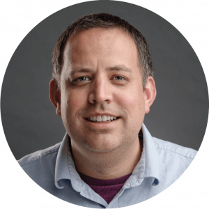
Ryan Murdick, Ph.D., Cryogenic Product Development Scientist, FormFactor, Inc.
Dr. Ryan Murdick has worked in cryogenic instrumentation for more than a decade; specifically, Scanning Probe Microscopy. He has built more than 25 custom SPM systems for cryogenic environments. Past employers include Montana Instruments and RHK Technology and he has consulted for Quantum Design, Prime Nano, and Molecular Vista. Dr. Murdick earned a PhD in Physics from Michigan State University in the field of Ultrafast Electron Diffraction and was a postdoctoral researcher at the University of Washington in the field of Nano Optics.
Single Sweep Broadband S-Parameter measurements for Semiconductor Transistor and IC Test to 220 GHz
Available for on demand viewing
With the growing demand for consumer devices working in the mm-wave range, including 5G/6G and automotive radar, there is a growing need to enable measurements to go all the way to 220 GHz in a single sweep. Traditionally, measurements beyond conventional coaxial frequency limits often requires more than 1 measurement to cover the broader frequency range of interest, demanding the performance levels that are equivalent to conventional coaxial approaches.
In this webinar we will present a new optimized single sweep solution for S-parameters measurements from 900 Hz to 220 GHz. We will also discuss recent developments of RF probes, instrumentation, calibration standards, and techniques that allow easy, accurate, repeatable, and trustworthy data.
Speakers
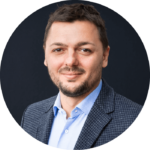
Giancarlo De Chirico | RF Market Segment Director at FormFactor Inc.
Giancarlo De Chirico is the Director of Marketing for the RF Market in the Probe Systems Business Unit at FormFactor. He has 11 years of experience in network analysis and characterization of RF, microwave, and mm-wave devices. He has hosted numerous seminars and workshops on component characterization techniques.
Before joining FormFactor, Giancarlo served as a Director at Keysight Technologies and was responsible for the growth of the Aerospace & Defense Device/Component Test and Military ATE industries. He holds a Master's Degree in Electronics Engineering from Politecnico di Milano (Italy) and a Bachelor's Degree in Electronics Engineering from Politecnico di Bari (Italy).
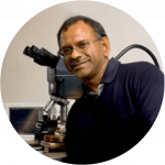
Suren Singh | Technical Lead Emerging Technologies at Keysight Technologies
Suren Singh received his BSEE from University of Durban-Westville, Durban South Africa in 1985. He completed a Graduate Diploma at the University of Witwatersrand, Johannesburg South Africa in December 1992. He then went on to complete his MSEE at the University of Witwatersrand, Johannesburg in 1995. Suren has been with the Hewlett-Packard Company, Agilent Technologies and now Keysight Technologies since 1986. His experience includes application engineering, product design, manufacturing, and test process development for microwave hybrid microcircuits. He also held the position of an application specialist and system architect, focused on the terahertz measurement solutions for Keysight. In addition, he is responsible for the metrology products for performance network analyzers, including both calibration and verification as applied to both ambient
and cryogenic temperatures. More recently Suren has been appointed as the technical lead for the emerging technologies for Quantum and 6G focused on the aerospace industry. More recently Suren has been involved in the development of solutions for cryogenic component testing for the Quantum based systems. He is also working closely with the industry leaders in millimeter wave space to bring to market solutions focused on 6G component characterization.
Strategies for Enabling Quantum Development with Test and Measurement from 77K down to milli-Kelvin
Available for on demand viewing
Quantum computing will likely utilize numerous new technologies which operate at different cryogenic temperatures. For example, a quantum computer might deploy CMOS memory modules at 77K, superconducting control chips at 4K, and a quantum processing unit (QPU) at less than 20 mK. To develop and deploy these various subsystems and technologies, it is vital to reliably and efficiently test and measure them at or near their operating temperatures.
Join this webinar to learn about:
- Technologies being explored at 77K, 4K, and milli-Kelvin for deployment in a quantum computer
- Challenges faced by researchers when performing cryogenic characterization measurements
- The leading solutions to measure cryogenic device and circuit performance at the wafer-scale and chip-scale.
About the hosts:
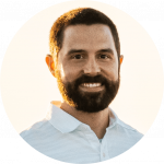
Jack DeGrave, Business Development Scientist in Quantum Technologies, FormFactor Inc.
Jack DeGrave joined the FormFactor-HPD Business Development team in early 2021 where he has focused on engaging with the Quantum Development Community members to map out the needs for cryogenic test and measurement, high density I/O device interfacing, and cryostats for deployment of quantum processors. His background in cryogenic test and measurement dates to early 2010 during his PhD studies in low temperature transport properties of helimagnets and skyrmions at the University of Wisconsin-Madison. After graduating, he held business development positions at several cryogenics companies. Jack brings greater than a decade of experience in cryogenic system design and test & measurement.

Thomas Funke, Senior Manager, Cryogenic Systems Product Marketing
Thomas Funke is a senior manager for cryogenic systems product marketing at FormFactor. Prior to this he worked for 10 year in cryogenics as a Research Scientist and authored 13 publications about cryogenic engineering and thermal insulation.
Thomas is a 2006 graduate of Technische Universität Dresden in Mechanical Engineering. In 2020 he received a PhD in cryogenic hydrogen storage from the TU Dresden and joined FormFactor. Within this studies he spend 1 year at the Vibration and Acoustics laboratories at Virginia Tech where he worked on active noise cancellation and interior aircraft noise control.
Superconductor and Spin Qubit Pre-Screening - Accelerate Quantum Development
Available for on demand viewing
FormFactor and Keysight invite you to learn how to speed development cycles for advanced quantum development. The companies have collaborated to develop an integrated measurement solution for pre-screening qubit devices at mK temperatures. The solution eliminates wire-bonding and packaging from cryogenic test processes to provide critical qubit performance parameters at 50 mK, enabling streamlined deployment in existing dilution refrigerators at 10 mK to reduce development cycle times by more than 2X. The turnkey measurement solution is fully optimized for qubit pre-characterization applications which removes the time-consuming process of selecting and integrating each individual piece of equipment.
Join this webinar to learn about:
- Technologies being explored at 77K, 4K, and milli-Kelvin for deployment in a quantum computer
- Challenges faced by researchers when performing cryogenic characterization measurements
- The leading solutions to measure cryogenic device and circuit performance at the wafer-scale and chip-scale.
About the hosts:

Jack DeGrave, Business Development Scientist in Quantum Technologies, FormFactor Inc.
Jack DeGrave joined the FormFactor-HPD Business Development team in early 2021 where he has focused on engaging with the Quantum Development Community members to map out the needs for cryogenic test and measurement, high density I/O device interfacing, and cryostats for deployment of quantum processors. His background in cryogenic test and measurement dates to early 2010 during his PhD studies in low temperature transport properties of helimagnets and skyrmions at the University of Wisconsin-Madison. After graduating, he held business development positions at several cryogenics companies. Jack brings greater than a decade of experience in cryogenic system design and test & measurement.
Philip Krantz, Business Developer & Quantum Physicist, Quantum Engineering Solutions, Keysight Technologies
Philip is a Business Developer in the Quantum Engineering Solutions (QES) team at Keysight Technologies. In the team, he is working to expand the customer base of the quantum measurement software Labber, as well as providing hands-on expertise in quantum engineering. Philip is also the QES lead for customer and industry partnerships.
Prior to his appointment at Keysight, he received his PhD in experimental quantum physics at Chalmers University, in Sweden. He also spent three years as a post-doc in the Engineering Quantum Systems group at MIT, as well as two years as the scientific coordinator of the Wallenberg Centre for Quantum Technologies in Sweden.
Unattended RF Measurement and Calibration for 5G Device Characterization and More
Available for on demand viewing
New generations of 5G devices can have dozens of RF channels operating at high frequency, creating a need for a greater on wafer test volume. In engineering, more device tests are needed to support the expanded speed bands, increasing the workload to complete testing. How can test engineers manage the load? What if the probers could operate unattended -- start a test and measure during a whole shift, overnight, or even over the weekend? There is a real, hands-free solution that provides fast, accurate measurements with high throughput -- leading to more accurate design models and faster time to market.
Learn how an autonomous wafer probe system with integrated components from Keysight and FormFactor can:
- Automatically perform wafer and die soaks to get the probes quickly to consistent operating temperature
- Quickly and automatically clean probes and then calibrate at mmw frequencies without user input
- Adjust automatically to multiple probe-to-probe spacings for different device geometries in a single test run
- Monitor calibration drift and recalibrate on the fly when necessary
- Work seamlessly for full temperature range -60 to 175C operation using N5291A Solution, from Keysight technologies, providing single sweep operation of 900 Hz to 130 GHz, and beyond this using Virginia diodes Waveguide mini modules and waveguide probes
About the hosts:

Gavin Fisher | Senior Applications Engineer at FormFactor Inc.
Gavin Fisher is a member of the Centre of Expertise group at FormFactor, providing application support and technical services to FormFactor’s customers. With more than 2 decades of experience working with Cascade probe systems, and with his deep technical knowledge in a broad spectrum of applications such as high-frequency measurement, measurement automation, calibration and power device measurement, he educates and trains customers on best practices to achieve accurate measurement results. He has made several presentations at European Microwave Week, MOS-AK workshops, and Agilent/Keysight seminars.
Prior to joining FormFactor, Gavin served as a Mechanical Engineer at Alenia Marconi Systems. He holds an upper-second degree from Brunel University in Mechanical Engineering with electronic systems.

Suren Singh | Technical Lead Emerging Technologies at Keysight Technologies
Suren Singh received his BSEE from University of Durban-Westville, Durban South Africa in 1985. He completed a Graduate Diploma at the University of Witwatersrand, Johannesburg South Africa in December 1992. He then went on to complete his MSEE at the University of Witwatersrand, Johannesburg in 1995. Suren has been with the Hewlett-Packard Company, Agilent Technologies and now Keysight Technologies since 1986. His experience includes application engineering, product design, manufacturing, and test process development for microwave hybrid microcircuits. He also held the position of an application specialist and system architect, focused on the terahertz measurement solutions for Keysight. In addition, he is responsible for the metrology products for performance network analyzers, including both calibration and verification as applied to both ambient
and cryogenic temperatures. More recently Suren has been appointed as the technical lead for the emerging technologies for Quantum and 6G focused on the aerospace industry. More recently Suren has been involved in the development of solutions for cryogenic component testing for the Quantum based systems. He is also working closely with the industry leaders in millimeter wave space to bring to market solutions focused on 6G component characterization.