February 14, 2025
From 5G, IoT, and AI applications to advanced packaging and high-bandwidth memory (HBM), ensuring device performance and yield at the wafer level is a critical step in the semiconductor manufacturing process.
February 14, 2025
From 5G, IoT, and AI applications to advanced packaging and high-bandwidth memory (HBM), ensuring device performance and yield at the wafer level is a critical step in the semiconductor manufacturing process.
As semiconductor devices continue to evolve in complexity, the demand for precise and reliable wafer test solutions has never been higher. From 5G, IoT, and AI applications to advanced packaging and high-bandwidth memory (HBM), ensuring device performance and yield at the wafer level is a critical step in the semiconductor manufacturing process.
Wafer testing is an essential process in semiconductor manufacturing, as it helps identify defects early, ensures electrical performance, and optimizes yield. By implementing effective wafer-level test strategies, semiconductor manufacturers can reduce costs, improve device reliability, and accelerate time-to-market.
The Role of Wafer Testing in Semiconductor Manufacturing
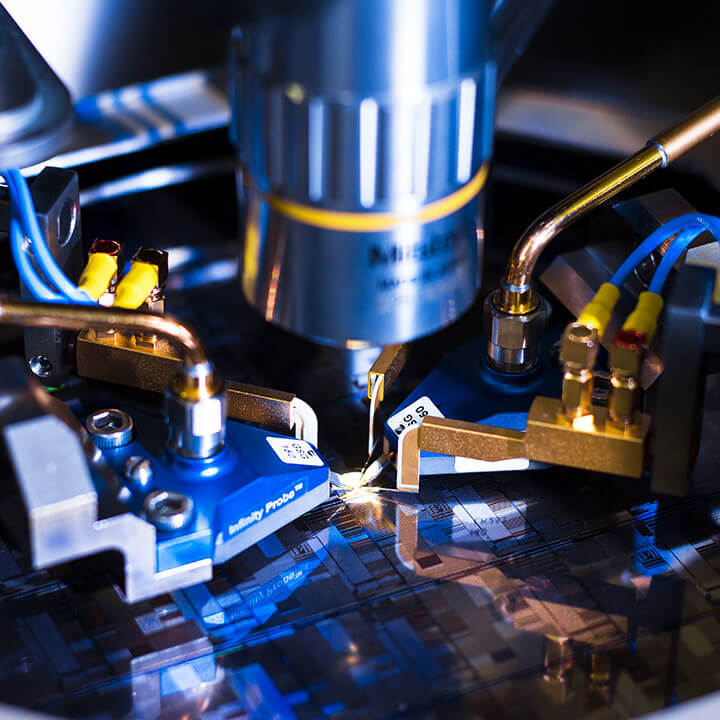
Wafer test is the process of testing semiconductor devices at the wafer level before they are diced and packaged. This step allows manufacturers to detect and isolate defective dies early in the production process, reducing waste and improving overall efficiency. Wafer-level testing is performed using probe cards that establish electrical contact with the die pads or bumps, enabling automated test equipment (ATE) to assess the device’s electrical characteristics.
Key Objectives of Wafer Test
Wafer test is especially critical for advanced semiconductor technologies, where process variations and fabrication defects can significantly impact device performance. As chip architectures become more complex, testing techniques must evolve to address new challenges.
5 Challenges in Wafer Testing and How to Overcome Them
1 ) Testing Advanced Nodes
As semiconductor manufacturers move to process nodes of 3nm and below, the ability to accurately measure electrical characteristics becomes increasingly difficult. Smaller transistor dimensions result in higher leakage currents, increased variability, and tighter process control requirements. Wafer test solutions must be capable of handling these challenges with precision probing, high-resolution measurement capabilities, and low-contact resistance probe technologies.
2 ) High-Volume Test Requirements
With more smart devices, electric cars, and cloud computing, the demand for semiconductors is skyrocketing. This requires higher test throughput without compromising accuracy. Multi-site probing, parallel testing, and automation play a critical role in enabling semiconductor fabs to test large volumes of wafers efficiently. Automated probe systems with robotic wafer handling and real-time data analytics can significantly improve throughput while maintaining high test accuracy.
3 ) Heterogeneous Integration and Advanced Packaging
New semiconductor architectures, such as chiplets and 3D ICs, present additional wafer test challenges. Unlike traditional monolithic designs, chiplet-based architectures require testing at multiple stages, including wafer-level, interposer-level, and package-level. Testing known-good-die (KGD) is crucial to ensuring yield and reliability in these advanced packaging approaches. Fine-pitch probing, high-speed signal integrity validation, and thermal management solutions are essential for effective wafer-level test in heterogeneous integration.
4 ) Cryogenic and High-Temperature Testing
As semiconductors are deployed in extreme environments, from deep space exploration to quantum computing, testing must be performed under specialized conditions. Cryogenic probe stations allow for wafer-level testing at temperatures as low as a few millikelvins, enabling the validation of superconducting qubits and other low-temperature applications. Conversely, high-temperature probe systems support automotive and industrial semiconductor testing, where devices must function reliably at temperatures exceeding 150°C.
5 ) Testing High-Speed and RF Devices
Modern semiconductor applications require high-frequency operation, particularly in 5G, Wi-Fi 7, and satellite communications. RF wafer test solutions must provide accurate signal characterization at millimeter-wave and terahertz frequencies. Advanced probe cards designed for high-frequency applications ensure precise S-parameter measurements and impedance matching, minimizing signal loss during testing.
3 Innovations in Wafer Testing for Next-Generation Devices
1 ) AI-Driven Wafer Testing
AI and machine learning are changing how we test semiconductors. AI-driven analytics can optimize test sequences, reduce test time, and identify defect patterns that traditional methods might miss. Predictive analytics enable fabs to make real-time adjustments to process parameters, improving yield and efficiency.
2 ) Automated Probe Systems
The integration of automation in wafer probe systems enhances test consistency and repeatability. Advanced probe stations equipped with precision motion control, automated optical inspection, and adaptive probe alignment reduce human intervention, minimizing errors and improving efficiency. These systems are particularly valuable for high-volume manufacturing environments where uptime and throughput are critical.
3 ) mmWave and Terahertz Testing
With the growing demand for high-speed communications and radar applications, semiconductor devices must be tested at frequencies exceeding 100 GHz. Wafer-level test solutions must incorporate highly specialized RF probe technologies, calibration techniques, and shielded environments to ensure accurate measurements at these extreme frequencies.
As a global leader in wafer test technology, FormFactor provides cutting-edge solutions designed to meet the evolving needs of semiconductor manufacturers. Our comprehensive portfolio includes:
With decades of experience and a strong focus on innovation, FormFactor is advancing wafer-level testing technology. This helps semiconductor companies develop high-performance devices with greater efficiency and reliability.
As semiconductor technology advances, wafer test will remain a critical step in ensuring device reliability, performance, and yield. The increasing complexity of chip architectures, the shift toward advanced packaging, and the rise of AI-driven test methodologies will drive further innovation in wafer-level test techniques. Manufacturers that leverage advanced test solutions will gain a competitive edge by reducing costs, improving yield, and accelerating time-to-market.
To learn more about how FormFactor’s wafer test solutions can help optimize your semiconductor manufacturing process, visit: FormFactor Wafer Test Solutions