As semiconductor devices get smaller and more complex, making sure they perform reliably is more important than ever. Parametric testing plays a key role in semiconductor development, providing the electrical measurements needed to validate designs, monitor fabrication processes, and optimize performance. With the right probe technology and automated test solutions, semiconductor companies can achieve greater precision, higher throughput, and better yield, all essential for staying competitive in today’s market.
What is Parametric Testing?
Parametric testing measures fundamental electrical properties, like resistance, capacitance, and current-voltage characteristics, on semiconductor wafers before they’re diced and packaged. These tests help engineers spot defects early, fine-tune manufacturing processes, and ensure devices meet performance standards.
Engineers rely on parametric testing to:
- Check semiconductor material quality – Every chip starts with a wafer, and its electrical properties must be just right. Parametric tests help confirm that the silicon (or other materials) has the correct conductivity, resistivity, and carrier mobility, ensuring that chips perform as expected.
- Monitor variations in the fabrication process – Semiconductor manufacturing involves dozens of steps, from photolithography to etching and doping. Even small deviations can cause performance issues. Parametric testing helps catch process variations early, so fabs can adjust before bad wafers pile up.
- Improve yield and reduce waste – Identifying problem areas at the wafer level means manufacturers can make fixes before chips move further down the production line. This reduces costly rework and ensures only high-quality devices reach the market.
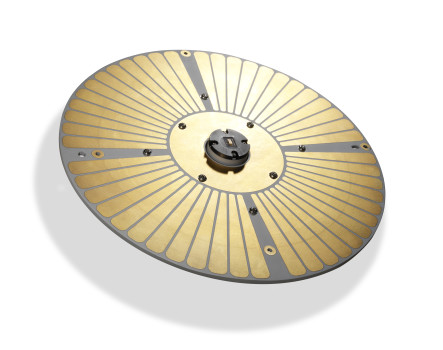
Why Probe Cards Matter in Parametric Testing
At the core of parametric testing are probe cards, which physically contact the wafer to measure electrical characteristics. FormFactor’s parametric probe cards stand out because they’re built for high precision, repeatability, and reliability.
- Precision that captures even the smallest variations – As chip features shrink to nanometer scales, measurements must be incredibly accurate. FormFactor’s probe cards minimize leakage and noise, so engineers get clean, reliable data.
- Low-leakage and low-capacitance performance – Modern chips operate at ultra-low power, meaning test systems need to detect extremely small electrical signals. FormFactor’s probes are optimized for low current leakage and minimal interference, enabling precise measurements even on the most advanced semiconductor nodes.
- Reliable contact technology that protects the wafer – Making electrical contact with delicate wafer structures is tricky. Too much pressure, and the wafer could be damaged; too little, and the connection is unstable. FormFactor’s MicroSpring® contact technology provides a stable, durable, and low-force connection that ensures accurate testing without harming fragile test pads.
Accuracy in Parametric Testing Matters
As semiconductor applications expand into areas like AI, 5G, automotive, and IoT, accuracy in parametric testing has never been more critical. Getting these measurements right impacts every stage of semiconductor development:
- Reliability and performance – If parametric tests aren’t accurate, faulty devices could slip through, leading to failures in the field. This is especially critical in automotive, aerospace, and medical electronics, where reliability isn’t optional, it’s mandatory.
- Yield optimization – Semiconductor fabs operate with razor-thin margins, and maximizing yield is essential. By catching process variations early, parametric testing helps fabs avoid costly scrap and rework. The result? More good chips per wafer, improving profitability.
- Faster time-to-market – Speed matters in the semiconductor industry. Reliable parametric test data means faster debugging, quicker product qualification, and a smoother production ramp-up, helping companies bring cutting-edge devices to market before the competition.
FormFactor Solutions for High-Volume Parametric Testing
FormFactor’s parametric test solutions are designed for high-throughput, high-accuracy semiconductor characterization. Whether you’re working with legacy nodes or pushing the limits with FinFETs, 3D ICs, or compound semiconductors, FormFactor’s test solutions deliver:
- Unmatched measurement accuracy – As semiconductor nodes shrink below 5nm, accurate testing gets harder. FormFactor’s probes are built for extreme precision, ensuring semiconductor companies can measure even the tiniest variations with confidence.
- Faster test times to improve efficiency – In high-volume manufacturing, every second counts. FormFactor’s optimized probe cards and automated probe stations reduce setup times, minimize variability, and speed up test cycles without sacrificing accuracy.
- Scalability for different device types – From traditional silicon chips to heterogeneous integration and chiplet architectures, FormFactor’s test solutions adapt to evolving semiconductor designs, ensuring long-term usability and cost-effectiveness.
Parametric testing isn’t just about taking measurements, it’s about ensuring the accuracy and reliability of the entire semiconductor development process. As devices become more advanced, the need for high-precision, high-throughput testing solutions continues to grow.
With FormFactor’s cutting-edge probe technology, automation solutions, and deep industry expertise, semiconductor companies can push the limits of performance while maintaining cost efficiency and quality assurance. Whether you’re working on next-generation AI processors, automotive-grade chips, or 5G RF devices, FormFactor delivers the parametric test capabilities needed to stay ahead of the curve.