Alan Liao, Director of Probe Product Marketing at FormFactor, presented at SEMICON Korea 2025 this week. Here’s a summary:
As semiconductor devices grow more complex, ensuring that each component functions correctly before integration is essential. With multi-chiplet architectures becoming standard, Known Good Die (KGD) testing plays a key role in improving final yield and reducing costs. This presentation explored how FormFactor’s latest advancements in high-speed wafer testing address the electrical and thermal challenges of KGD testing for next-generation memory devices.
With advanced packaging expected to account for over half of integrated circuits by 2025, the need for reliable KGD testing is greater than ever. The growing number of HBM layers, from 4 to 16, requires precise wafer-level testing to identify defects early, improve yield by more than 10%, and reduce manufacturing costs.
Addressing Key Testing Challenges
KGD testing must maintain signal integrity at high speeds while ensuring accurate thermal probe-to-pad alignment. Electrical challenges include minimizing insertion loss and maintaining consistent voltage swing at frequencies beyond 4 GHz. Mechanically, mismatches in the coefficient of thermal expansion (CTE) between probe cards and wafers can lead to misalignment during thermal cycling, impacting test accuracy.
Pushing the Limits: High-Speed Performance Beyond 4 GHz
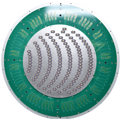
FormFactor’s HFTAP K40 probe card, designed for advanced memory testing, delivers minimal insertion loss of -3 dB at 7 GHz, supporting HBM4, LPDDR6, and GDDR7 technologies. Ongoing R&D aims to extend performance beyond 5 GHz, ensuring readiness for future high-speed memory devices.
Optimizing Thermal Probe-to-Pad Alignment
Thermal misalignment can reduce test reliability, especially as HBM wafers heat up during testing. FormFactor addresses this with design optimizations:
- Wafer-Side Stiffener: Matching the CTE of the stiffener to the wafer ensures a slower temperature response, improving alignment by 40% compared to ceramic substrates.
- DUTLet Base Design: Precise DUTLet placement reduces CTE scaling errors to ~65 ppm, compared to 105 ppm with traditional designs, maintaining alignment throughout the test cycle.
- Enhanced Local Planarity Adjustment: With three times more local adjustment points, the probe card maintains a consistent Z-profile, ensuring reliable contact across the wafer.
FormFactor’s HFTAP Matrix Probe Card represents a breakthrough in high-speed wafer testing, addressing both electrical and thermal challenges to support KGD testing for next-generation memory devices. By enabling faster data rates with minimal signal loss and maintaining precise alignment, this technology helps semiconductor manufacturers achieve higher yields and lower production costs as they push the boundaries of advanced packaging.