July 19, 2024
Mike Slessor, FormFactor CEO, discusses silicon photonics testing complexity and impact on data center power consumption in the Mission Central video below – Testing Silicon Photonics and Its Critical Role in Modern Data Centers.
July 19, 2024
Mike Slessor, FormFactor CEO, discusses silicon photonics testing complexity and impact on data center power consumption in the Mission Central video below – Testing Silicon Photonics and Its Critical Role in Modern Data Centers.
Silicon photonics essentially brings together two advanced technologies—integrated circuits (ICs) and optical communications—that have traditionally developed on separate tracks. Each has its unique benefits: silicon-based IC fabrication can integrate billions of transistors onto a single chip, while laser-based optical communications deliver extremely high bandwidths and low-loss signal transmission over long distances. When combined through silicon photonics, these technologies unlock new potentials in transmission speed, scalability, energy efficiency, and cost reduction. Over time, silicon photonics is expected to evolve from data center applications to interconnects on individual chips. Eventually, it’s possible that hundreds of cores on a single IC could be interconnected using an on-chip optical mesh.
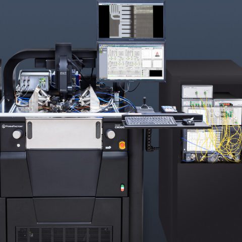
Our line of silicon photonics products includes a fully automated test system equipped with advanced hardware and software for rapid, adaptive fiber array probe positioning. The CM300xi-SiPh probe system is specifically designed for high-volume research and development as well as niche production of silicon photonics wafers.
This includes:
Mike Slessor, FormFactor CEO, discusses silicon photonics testing complexity and impact on data center power consumption in the Mission Central video below – Testing Silicon Photonics and Its Critical Role in Modern Data Centers.