We have a new on demand webinar now available – Next Generation DC Probes for Accurate and Repeatable Device Modelling Measurements. This webinar is presented by Conner Smith, Principal Applications Engineer at FormFactor.
The semiconductor industry is experiencing relentless downscaling of gate length and the evolution of new architectures for silicon-based transistors, reaching sizes of 2 nm and beyond. Advanced transistors at this scale exhibit increased on-state currents as supply voltages decrease, while maintaining low off-state currents to minimize power consumption.
Challenges arise due to smaller test pads aimed at reducing lithography costs and the use of copper backend metallization, which makes achieving low and stable contact resistance for probes difficult. This challenge becomes more pronounced, especially at elevated temperatures, when probed aluminum cap layers on the pads oxidize rapidly, hindering the ability to establish reliable probe contacts.
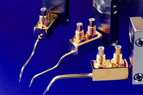
In this presentation, we introduce the next generation of advanced guarded DC probes. These probes feature small scrubbing areas, low leakage performance, and true Kelvin force-sense probe tips to effectively address the testing challenges associated with making precise and consistent wafer measurements for device modeling.
Connor works out of our Boulder, CO cryogenic lab. His main function is to help customers to solve their testing problem through configuration of products or test services. While Connor started in the cryogenic lab at FormFactor, he currently supports the probe systems business unit.
Prior to working at FormFactor, Connor was active during his years as a student at Colorado School of Mines where he worked as a lab assistant and community director while studying mechanical engineering.