September 19, 2024
FormFactor's probe cards, such as Apollo and Kepler™, are engineered to address these challenges, offering precise contact and measurement capabilities that ensure defect-free production and optimized yields.
September 19, 2024
FormFactor's probe cards, such as Apollo and Kepler™, are engineered to address these challenges, offering precise contact and measurement capabilities that ensure defect-free production and optimized yields.
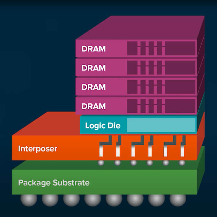
In recent years, advanced packaging technologies have seen significant growth, with High Bandwidth Memory (HBM) emerging as a major revenue driver for memory manufacturers. Utilizing 2.5D and 3D packaging, HBM presents unique challenges, especially when using probe cards for Known Good Die (KGD) testing. As HBM3e pushes data transfer rates (up to 9.6 GT/s) and incorporates more stacked dies, managing power consumption and heat dissipation becomes increasingly complex. Addressing these issues requires thermally optimized MEMS technology to maintain stable probe-to-pad alignment during testing.
Semiconductor wafer testing is integral to the production and performance of HBM, which is essential for applications like artificial intelligence (AI), machine learning, and data centers. HBM requires advanced testing due to its stacked architecture, tight integration, and need for high-speed data transfer. FormFactor’s probe cards, such as Apollo and Kepler™, are engineered to address these challenges, offering precise contact and measurement capabilities that ensure defect-free production and optimized yields.
The importance of quality assurance during HBM manufacturing is critical. With increasingly complex designs, ensuring every die’s functionality is vital to the overall performance of HBM modules. The use of advanced wafer testing improves production efficiency and minimizes costs by catching defects early in the process. FormFactor’s innovative testing solutions thus play a pivotal role in maintaining the reliability and scalability of semiconductor technologies crucial to modern computing.
Mike Slessor, FormFactor CEO, discusses the role of semiconductor wafer test in high bandwidth memory in the Mission Central video below – High Bandwidth Memory – Testing a Key Component of Advanced Packaging – NEW VIDEO