Prolonged delays in obtaining data can impede the progression of development cycles and disrupt production timelines. Utilizing cryogenic test services can help you sidestep the significant initial capital expenses associated with a full system, facilitate prompt access to cryogenic data, and guarantee that you acquire the critical data necessary for propelling your project forward.
Come to the Cryogenic Test Lab in Boulder, Colorado, and collaborate with FormFactor to develop tailored probing solutions and gather essential cryogenic data for your needs.
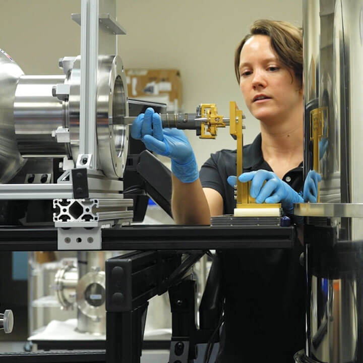
The Test Lab can provide a variety of services and accessories designed to meet your cryogenic testing needs. Our offerings include singulated die characterization at temperatures below 50 millikelvin and high-throughput wafer probing within a range from below 4 Kelvin up to 77 Kelvin. For setting up tests of varying complexity, we offer engineering services billed at an hourly rate. Our senior scientists are available to consult on your testing plans and assist with intricate measurements. Additionally, we offer customizable cryogenic probes and probe cards for both DC and RF measurements (exceeding 20 GHz), tailored to fit your device layout and testing requirements.
Custom Chip Scale Testing
Singulated dies and packaged devices can undergo testing in cryogenic conditions as low as 50 millikelvin. This service is particularly suited for low-volume testing, application development, and material characterization. We offer a comprehensive selection of standard probes and sockets, with options for custom probes, fixtures, and cables available for an additional fee.
Testing is performed using a Model 106 ADR cryostat, which employs a two-stage Adiabatic Demagnetization Refrigerator (ADR) to reach a baseline temperature of 50 millikelvin. This system also features a sizable 4 Kelvin plate and multiple signal feedthroughs. Example measurements include prescreening superconducting qubits using dispersive readout, testing low-noise amplifier (LNA) components, and determining superconducting transition temperatures.
Custom Wafer Scale Testing
Full-scale wafers can be tested at temperatures as low as 4 Kelvin utilizing fully automated probe movement. This service is ideal for high-volume, rapid measurements on 150 mm and 200 mm wafers. The testing environment is optimized for superconducting devices through the use of two layers of magnetic shielding. You can quickly start with our standard probe cards, or opt for a custom probe card, which can be made for an additional fee. Automation capabilities allow measurements to continue uninterrupted overnight and throughout weekends, maximizing testing efficiency.
Testing is carried out on an IQ3000 Cryogenic Wafer Prober, which features manual wafer exchange and employs closed-cycle cryocoolers to maintain base temperatures, eliminating the need for helium dewar exchanges typical of wet systems. Example applications include parametric testing of superconducting (SC) flux quantum (SFQ) circuits, readout resonator screening for superconducting qubit circuits, and ultra-low noise (ULN) measurements of random telegraph signals (RTS) on read-out integrated circuits (ROIC).
Coming soon… Low noise figure component testing.
For more information, explore a video walkthrough of the Cryogenic Test Lab.