As the demand for advanced package IC’s dramatically increases, KGD test solutions require better test efficiency to reduce cost and support higher volume. Coupled with the advancement of DRAM and High Bandwidth Memory (HBM) native speed capability, the latest memory is running beyond 2 GHz (4 Gbps) which is pushing the limit on existing ATE testers. Recent joint efforts between FormFactor and industry leaders successfully demonstrated that testing beyond 3 GHz is achievable.
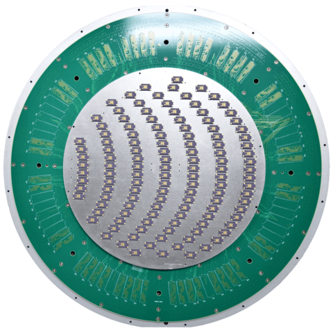
The HFTAP K32 Probe Card Solution
The extended capability of FormFactor’s HFTAP K32 probe card architecture enables DRAM customers on wafer-level speed testing up to 3.2 GHz/ 6.4 Gbps for next generation known-good-die (KGD) memory. The recent industry-wide adoption of heterogeneous integrated systems enabled by 2.5D and 3D advanced packaging technology is driving the demand for KGD. The benefit of KGD testing ensures the final stacked and assembled package does not get scrapped due to one bad chip.
This advanced MEMS probe card architecture is used to verify electrical performance and yield, not only for the individual chips, but also devices used in the HBM stack, including the fine-pitch interposer to ensure the performance of the complete package. The HFTAP K32 probe card solution empowers customers to gain more intelligence at any stage of the heterogeneous integration process for advanced packages, where the traditional way to optimize yield on a monolithic silicon die is no longer adequate.
Features and Benefits for Consideration
High-speed known-good-die (KGD)
- K32 (up to 3.2 GHz/6.4 Gbps) high-speed test capable at wafer level
- Supports advanced packaging requirements for at speed testing
- Enables testing of latest generation memory products, including LPDDR4X, DDR5, LPDDR5, HBM3, GDDR5, and GDDR6
Stable test temperature performance
- Operates at a wide temperature range
- Utilizes production proven SmartMatrix™ platform with 440 mm/ 520 mm PCB size
T11.x spring reliability
- Scalable 3D MEMS MicroSpring™ technology enables flexible pad layout with superior contact performance and delivers long probe card lifetime
- Excellent current-carrying capacity
- Fine pitch capability down to 50 μm
- Able to probe on very small pads
Ease of use and serviceability
- Real-time planarity adjustment and optimization capability with probe card on the test cell
- Regional single spring repair and probe head replacement capability reduces time loss for service events and improves equipment efficiency
To learn more about the HFTAP K32 Probe Card solution visit the website and download the datasheet.