August 10, 2023
Testing VCSEL devices and on-wafer μLED present several formidable challenges. An essential demand involves conducting single and dual-sided testing, which encompasses probing from either the front or backside of the wafer.

August 10, 2023
Testing VCSEL devices and on-wafer μLED present several formidable challenges. An essential demand involves conducting single and dual-sided testing, which encompasses probing from either the front or backside of the wafer.
The VCSEL market is experiencing remarkable growth due to fresh opportunities arising in smartphone and automotive sectors. Notably, VCSELs are finding novel applications in these domains. In smartphones, the pivotal role of 3D sensing for facial recognition has led to the integration of up to three VCSEL dies within a single device. Meanwhile, the automotive realm is witnessing the emergence of applications like driver monitoring, infotainment control, and LiDAR, which are set to further amplify the VCSEL market’s expansion.
 As VCSEL-enabled 3D sensing continues to explore new avenues, the technology’s impact on our daily lives is profound. It contributes to heightened security, enhanced safety, and increased intelligence in the devices we rely upon regularly.
Like with the VCSEL market, MicroLED (μLED) display technology is gaining escalating interest and is on the brink of making its presence felt in consumer goods. The horizon for μLED displays is broadening, encompassing a range of burgeoning applications including wearables, smartphones/tablets, televisions, and virtual/augmented reality (VR/AR) environments, as well as the automotive sector. In contrast to other display technologies such as OLED and LCD, μLED displays stand out with their superior attributes. These include enhanced resolution, an expansive dynamic range, swifter response times, and reduced power consumption, resulting in extended battery life.
Testing VCSEL devices and on-wafer μLED present several formidable challenges. An essential demand involves conducting single and dual-sided testing, which encompasses probing from either the front or backside of the wafer. To handle thin, non-flat wafers like GaAs, InP, and others of sizes 4″ and 6″, the probe system must exhibit adeptness in wafer handling.
Given the circumstance that traditional thermal chucks are unsuitable for dual-sided wafer probing, achieving accurate cool-to-hot dual sided testing necessitates the incorporation of a localized cooling/heating source within the measurement setup.
The intricacy of the testing process is compounded by an intricate suite of measurements, including far-field, near-field, and light-I-V (LIV) evaluations. Conducting these measurements demands a variety of optics and detectors, each of which entails distinct test setups and iterations to complete the measurements satisfactorily.
Additionally, when dealing with multi-side testing, both the design of the probe card and the control of the Device Under Test’s (DUT) temperature become notably more intricate and demanding.
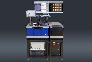
 FormFactor addresses these challenges with a range of dedicated manual, semi- and fully automated probe stations for high-precision single and dual-sided optical on wafer measurement. The PA200 BlueRay™, available in variety of configurations, enables high-throughput functional testing of optoelectronic components. The system may be equipped with a patented, thermally controlled probe unit, that enables test for both high and low temperature with very stable and accurate conditions. It also offers special optics to measure light intensity, current and voltage, and manual or motorized positioners for double-sided probing.
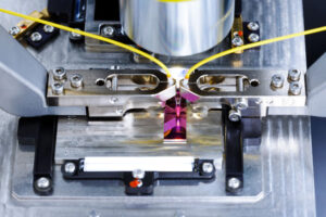
For researchers involved in the development of new devices, the MPS150-SiPh is a cost-effective, manual measurement solution. The MPS150-SiPh allows precise alignment of optical fibers to facilitate the ingress and egress of light from a device, all accomplished without any physical contact. Benefiting from its user-friendly design, the MPS150-SiPh stands as an ideal choice for those new to the field, offering a platform to explore photonics while attaining unparalleled precision in test outcomes. For more information on the MPS150-SiPh, download the Overview.
From lab to fab, FormFactor solutions are tailored to test optical electronics. In manufacturing production, FormFactor’s Akari probe cards, with both multi-site and single-site/2-pin options, deliver a high-precision test solution for LEDs and μLEDs. Akari’s excellent 3D MEMS spring stability ensures contact accuracy over millions of touchdowns.