February 26, 2021
Components and measuring tasks in 3D surface metrology are becoming more and more complex. Certain measurement tasks can no longer be solved by a single sensor, and these situations call for hybrid metrology.

February 26, 2021
Components and measuring tasks in 3D surface metrology are becoming more and more complex. Certain measurement tasks can no longer be solved by a single sensor, and these situations call for hybrid metrology.
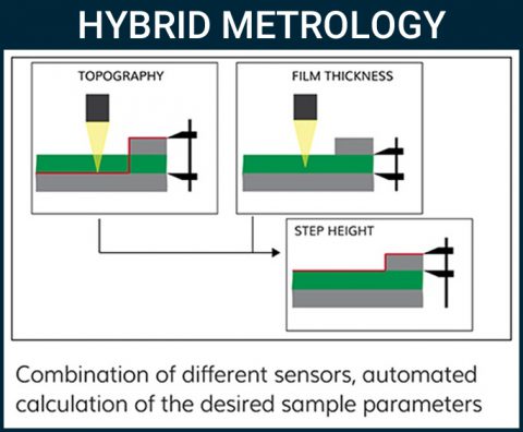
Components and measuring tasks in 3D surface metrology are becoming more and more complex. Certain measurement tasks can no longer be solved by a single sensor, and these situations call for hybrid metrology. Modern 3D surface measuring tools can combine several measuring principles by different point, line, field of view and layer thickness sensors in one device. This makes it possible to solve a measuring task with different sensors by carrying out a measurement with each sensor. The different results are then combined with each other. Learn more about our multi-sensor technology SurfaceSens.
FormFactor’s FRT Metrology Systems were highlighted in a 3DInCites article – Diversification of Markets Calls for Hybrid Metrology with Multi-Sensor Technology. The article pointed to the need for hybrid metrology for advanced packaging:
Despite continued efforts to scale CMOS structures to smaller nodes, metrology needs are fairly straightforward thanks to standardization of tools and processes. This is not the situation for metrology in the advanced packaging space. Measuring total thickness variation (TTV) on a wafer is not the same as measuring TTV with a very high lateral resolution. Additionally. through silicon vias (TSVs), Cu bump or pillar heights, as well as thinning, bonding and stacking are bringing new metrology needs compared to classical process steps.
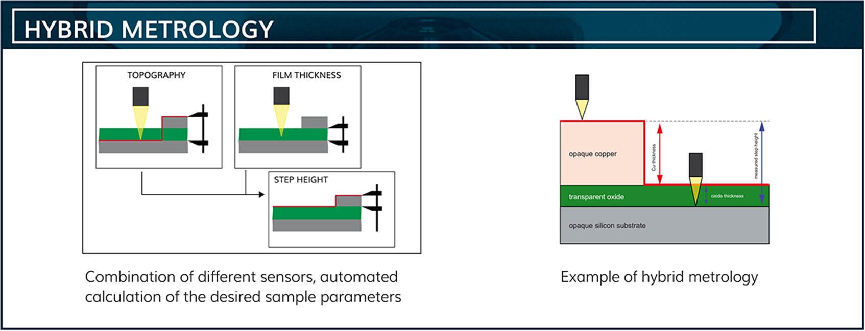
One example of how hybrid metrology works is in determining the copper layer thickness which is not physically measurable. See the example below:

Here, the layer stack is located on a wafer (opaque silicon substrate), a transparent oxide layer on top of it and an additional opaque copper layer in a limited area. If an optical topography sensor is used to measure the step height of the copper layer it actually measures the common step height of the opaque copper layer and the transparent oxide layer. In order to determine the thickness of the copper layer, a topography sensor is used to measure the thickness of the copper layer, including the transparent oxide layer. Furthermore, the thickness of the transparent oxide layer is measured separately with a film thickness sensor. By subtracting the oxide thickness from the total thickness determined previously, the desired step height of the copper layer is obtained.
For the measurement of topography, roughness, sample thickness, layer thickness and many other surface parameters, the FormFactor FRT surface measuring systems can be equipped with various sensors. FormFactor FRT offers a wide range of point, area and film thickness sensors and even an Atomic Force Microscope (AFM), which are fully integrated into the tool and can be flexibly arranged and combined. The possibility of retrofitting sensors opens up further options for flexible adaptation to future measuring tasks, such as individual and exchangeable sample holders.