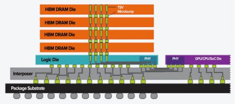
In a heterogenous Integrated system, the impact of composite yield fallout due to a single chiplet is creating new performance imperatives for wafer test in terms of test complexity and coverage. From a test perspective, making chiplets a mainstream technology depends on ensuring Good Enough Die at a reasonable test cost.
Wafer-level test plays a critical and intricate role in the chiplet manufacturing process. Take the case of HBM (High Bandwidth Memory), it enables early identification of defective DRAM and logic dies so that they can be removed before the complex and expensive stacking stage. Further testing of the post-stack wafer ensures the full functionality of completed stacks before dicing them into stand-alone assemblies. Ideally, each DRAM chip would be subjected to a Known Good Die (KGD) test to independently validate its performance prior to stacking. But that’s often not economically feasible. At some point, the cost of test outweighs the value added when the system is completed.
Therefore, a test strategy to balance the test cost and the cost of undetected yield fallout is needed to bring heterogenous integration to high-volume production. Thanks to innovations in MEMS probe card technology, FormFactor’s products help customers mix-and-match between full test coverage KGD test flow (such as the Altius™ probe card that supports 45μm grid-array pitch microbump probing for at-speed HBM and interposer validation) and high-throughput test flow with acceptable risk for limited test (such as the SmartMatrix™ probe card that dramatically reduces test cost per die by testing thousands of die on a 300mm wafer simultaneously).
Ultimately, we help customers lower overall manufacturing cost, by gaining more intelligence on device performance and yield at every stage of the chiplet manufacturing process.
Amy Leong
Chief Marketing Officer
FormFactor, Inc.
