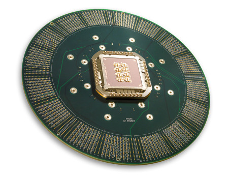
Foundry and Logic Applications
AI, HPC, and the growth of consumer electronics are advancing next-generation logic technologies. FormFactor’s wafer probe cards deliver precision and efficiency to meet the evolving test challenges.
The semiconductor industry is at a pivotal moment, driven by rapid advancements in Artificial Intelligence (AI), High-Performance Computing (HPC), automotive technology, and mobile devices. As devices become smaller, more powerful, and interconnected, the demand for high-performance, reliable testing solutions is greater than ever. To meet these challenges, FormFactor’s foundry and logic wafer probe cards are designed to provide the precision and scalability needed for next-generation semiconductor testing.
As the volume of data generated by internet traffic and diverse sources continues to surge, the demand for faster, more efficient server processors and real-time AI capabilities escalates. Simultaneously, the rise of wearables, smartphones, and the Internet of Things (IoT) is pushing the need for compact, high-performance devices with extended battery life. Logic chips powering these devices are increasingly packaged in smaller form factors, utilizing wire bond, flip-chip, and wafer-level packaging. Additionally, the automotive sector’s expanding use of semiconductors requires devices to meet stringent reliability and safety standards, along with wider temperature tolerance ranges.
Many of these devices integrate semiconductor logic or CPUs into Systems on Chips (SoCs) to enable their unique functions. To keep pace with these advances, semiconductor manufacturers are under constant pressure to reduce the total cost of testing. A key strategy to reduce testing costs is to eliminate unnecessary packaging of defective devices by conducting functionality and performance tests at the wafer level, known as “sort test.” A crucial element of this cost reduction is increasing the number of die tested in parallel. For flip-chip and wire-bond applications, this requires expanding the active area while maintaining stringent electrical performance and fine pitch requirements, which in turn increases probe card design complexity.
To meet these evolving challenges, vertical probe card solutions must adapt both in terms of architecture and probe design. Probe card architectures must be engineered to handle thermal and mechanical stresses while supporting the electrical performance required to meet device testing standards and higher spring count demands.
Testing Advanced Packaging ICs
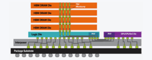
As companies adopt advanced packaging techniques, there is a growing need for cost-effective, scalable testing solutions that can support high-volume production. These advanced packages, which integrate multiple device types—such as memory and logic—into high-performance systems, present unique challenges that require specialized probe card technologies.
Techniques like 2.5D and 3D stacking are transforming the semiconductor landscape by merging diverse chip types into compact, high-performance systems. Testing these complex packages becomes particularly challenging when probing microbumps and Through-Silicon Vias (TSVs) at extremely fine pitches.
One significant challenge is testing the interposers that interface the various components within the package. The logic layer, typically fabricated on a separate wafer with microbumps, serves as the foundation for stacking additional components. After stacking, the wafer is tested by probing the exposed microbumps on the logic die. With microbumps as small as 25μm in diameter and pitches down to 45μm, these dense arrays—sometimes numbering up to 4000—pose both mechanical and electrical testing challenges, as they carry data, power, and ground.
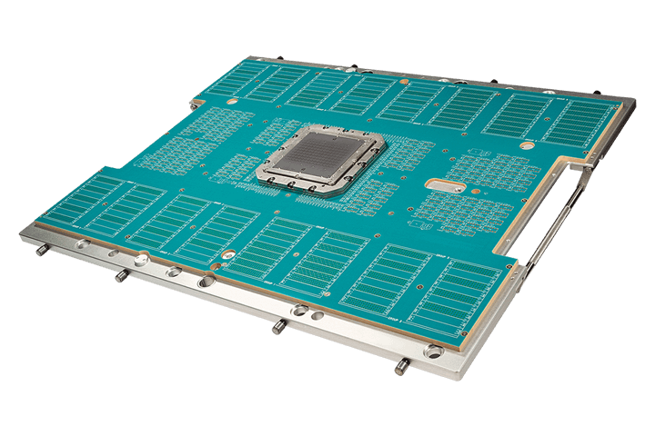
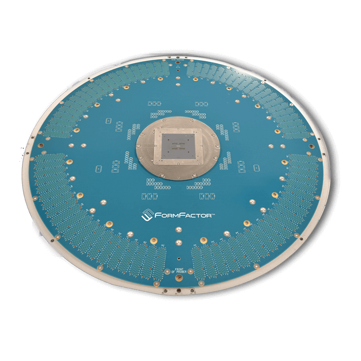
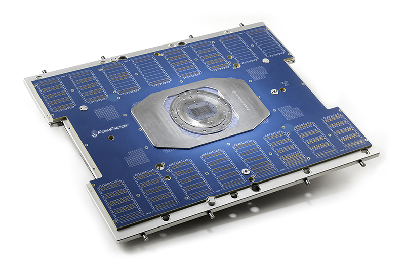
FormFactor provides advanced testing solutions that balance cost, performance, and coverage. Our Altius™ probe card, for example, supports microbump pitch testing as fine as 45μm and enables high-speed verification of >3Gb/s. Through continuous collaboration with IC manufacturers and Automated Test Equipment (ATE) providers, we develop solutions that keep pace with the rapid evolution of advanced packaging. Our approach integrates composite metal MEMS probes and hybrid MEMS designs into our probe cards, delivering finely tuned pitch, enhanced current-carrying capacity, and reduced power impedance.
Meeting High Throughput Demands for Faster Time-to-Market
As the demand for faster, more powerful semiconductors accelerates, manufacturers are under pressure to reduce time-to-market while maintaining product quality. By increasing the parallelism of testing, FormFactor’s solutions enable manufacturers to test multiple dies simultaneously, reducing the cost of test and improving throughput. This high-parallelism approach ensures that more devices are tested in less time, driving efficiency and faster production cycles. Achieving high throughput in testing not only reduces overall test costs but also ensures the timely release of next-generation products, a critical factor in today’s fast-moving technology markets.
Bump/Cu Pillar Probing for HPC, Artificial Intelligence, Applications Processors and Server Chips (GPU, CPU)
For high-current, multi-DUT testing applications, such as AI processors, application processors (APs), and server chips, FormFactor’s Apollo™ vertical probe card delivers a high current-carrying capacity of >1.8A per probe. Apollo™ offers outstanding reliability and scalability, addressing a wide range of testing requirements while maintaining exceptional electrical and mechanical performance.
Apollo™ is widely used for baseband and application processor testing in mobile devices, known for its “Right First Time” reliability. Its unique electrical and mechanical design capabilities optimize yield in multi-site testing environments. Apollo™ also supports a variety of probe options, including traditional Cobra-style wires, fine-pitch vertical MEMS probes, and space transformer options, enabling a flexible configuration that minimizes test costs for mobile device testing.
Apollo™ is also the industry-leading probe card for flip-chip bump testing in high-end game consoles and consumer ICs, providing precision and reliability for multi-core processors.
As the semiconductor industry evolves, so too will the demands for more advanced, efficient, and scalable testing solutions. At FormFactor, we remain committed to pushing the boundaries of probe card technology, continuously developing innovations that meet the growing challenges of AI, automotive, HPC, and beyond. With a focus on precision, scalability, and cost-efficiency, we are poised to support the next generation of semiconductor breakthroughs.