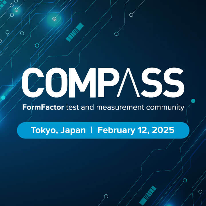
COMPASS, The FormFactor test and measurement community, will be in Tokyo, Japan on Wednesday, February 12, 2025, at the Tekko Executive Lounge and Conference Room. The Seminar runs from 11am – 17:10, with a reception to follow until 19:00. For complete venue details and agenda, please visit the COMPASS Japan website.
Here’s a sneak peak at some agenda break-out session highlights:
11:30 – 12:00 – Session #1: New Level Innovation of Advanced Heterogeneous Integration
Speaker: Takashi Kariya, Corporate Vice President / Head of Lab, Device Solutions R&D Japan Advanced Package Lab, Samsung Japan Corporation
This session will explore the advancements in heterogeneous chip packages essential for future innovations. Takashi Kariya will introduce Samsung’s AVP Platform, discussing its technology roadmap, challenges, and opportunities in high-end computing, memory, and mobile applications.
13:00 – 13:30 – Session #2: Wafer Probe Test Challenges and Solutions for Advanced SoC Devices and Applications
Speaker: Cameron Harker, Sr. Director, Business Development, FormFactor Inc.
As maintaining Moore’s Law becomes more challenging, this session will delve into solutions for increasing transistor density, developing larger devices, and reducing costs. Cameron Harker will review recent SoC device test trends, advanced packaging, and wafer test challenges, presenting unique probe solutions from FormFactor.
13:30 – 14:00 – Session #3: Importance of Current Noise for Low Noise Environments
Speaker: Masahiro Sameshima, Senior Staff Application Engineer, FormFactor Japan
Focusing on noise issues in wafer prober systems and measurement environments, Masahiro Sameshima will explain methods to assess noise levels and identify main sources, highlighting solutions implemented since 2010 to achieve low-noise environments.
14:30 – 15:00 – Session #4: Technology Evolution on Production Silicon Photonics
Speaker: Divya Pratap, Silicon Photonics Program Director, FormFactor Inc.
With silicon photonics testing moving rapidly into production, this session will discuss strategies to ensure exceptional reliability from wafer probing systems. Divya Pratap will address maintaining consistent operation under high pressure, scalability, throughput, and robustness to achieve efficiency and reliability in production environments.
15:00 – 15:30 – Session #5: FormFactor’s Probe Solutions for Next Generation DRAM Technology
Speaker: David Cooke, Sr. Product Marketing Manager, FormFactor Inc.
This presentation will cover how smaller DRAM geometries, advanced packaging, and higher interface speeds drive demand for robust testing capabilities. David Cooke will present FormFactor’s probe card technology designed to enhance test coverage, optimize yield, and accelerate mass production ramps for DRAM manufacturers.
16:00 – 16:30 – Session #6: Optimization of Test Strategies for Innovative Chiplets for AI/HPC Applications
Speaker: Shinji Fujita, Principal/Test Strategist, Advantest
As semiconductor technology evolves, especially with chiplets in AI/HPC applications, test processes require significant optimization. Shinji Fujita will discuss new Die-Level Test approaches and the importance of shifting test strategies to ensure yield improvement and quality assurance.
16:30 – 17:00 – Session #7: Maximizing OEE for High Volume Test: Innovative Probe Cleaning and Device Transport Solutions
Speaker: Dr. Jerry Broz, VP of Business Development & Strategic Marketing, Delphon Industries, Inc.
This session will highlight the importance of data integrity in wafer testing. Dr. Jerry Broz will discuss innovations in probe cleaning materials and device carriers that support reliable handling and cost-effective testing, emphasizing the need for collaboration and interdisciplinary problem-solving.
There will also be opening and closing speakers, lunch, and a closing reception to conclude the event. We hope to see you soon in Tokyo!