May 23, 2024
There’s a new paper from FormFactor that presents a novel coaxial guarded, true-Kelvin MEMS analytical DC probe with replaceable tips, which is introduced to achieve precise and consistent device modelling wafer measurements.
May 23, 2024
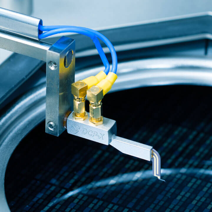
There’s a new paper from FormFactor that presents a novel coaxial guarded, true-Kelvin MEMS analytical DC probe with replaceable tips, which is introduced to achieve precise and consistent device modelling wafer measurements.
The semiconductor industry continues to pursue the relentless downscaling and development of new architectures for silicon-based transistor down to 2 nm and beyond. On state currents of such advanced transistors are increasing, while off-state currents are kept very low to reduce power consumption. Smaller test pads to reduce lithography and prototyping costs, and the use of copper backend metallization have increased the difficulties for probes to have low and stable contact resistance as there are inadequate fresh pad metal available for deeper probe scrubs or re-probing.
These issues aggravate especially at elevated temperatures when pad aluminum cap layer has been probed and removed, and the exposed underlying copper oxidizes, hindering the ability to establish consistently good electrical contacts for every probe touchdown. The popular quasi-Kelvin analytical DC probes, widely used in the industry, are not able to cope with these challenges.
There’s a new paper from FormFactor that presents a novel coaxial guarded, true-Kelvin MEMS analytical DC probe with replaceable tips, which is introduced to achieve precise and consistent device modelling wafer measurements. Despite recent low contact force and low contact resistance improvements on MEMS probe cards, they are excluded in the scope and discussions of this work because their probe tip layout is usually fixed, unable to support test structures with variable pad pitches.
There is also a webinar now available – Next Generation DC Probes for Accurate and Repeatable Device Modelling Measurements – where we introduce the next generation advanced guarded DC probes with small probe scrubs, low leakage performance and true Kelvin force sense probe tips to address the test challenges of making precise and consistent device modelling wafer measurements.