January 12, 2024
At the core of cutting-edge wafer probe cards lies the brilliance of MEMS, constituting approximately 75% of the global advanced probe card market. MEMS technology serves as the key to crafting probes with micron-level precision.
January 12, 2024
At the core of cutting-edge wafer probe cards lies the brilliance of MEMS, constituting approximately 75% of the global advanced probe card market. MEMS technology serves as the key to crafting probes with micron-level precision.
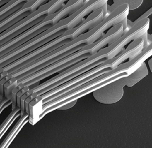
At the core of cutting-edge wafer probe cards lies the brilliance of MEMS (Micro-Electro-Mechanical Systems), constituting approximately 75% of the global advanced probe card market. MEMS technology serves as the key to crafting probes with micron-level precision, establishing contact with I/Os and power connections on ICs. This precision positions MEMS probes as ideal for supporting the intricate demands of fine-pitch and high-pin count requirements in leading-edge semiconductor process nodes and advanced packaging.
However, not all MEMS probes are crafted with the same level of excellence. Discover how FormFactor’s composite-metal MEMS technology is driving a spectrum of new ICs at the forefront of electronic innovations.
FormFactor’s MEMS probe cards are pioneering these innovations by tackling the challenges posed by advanced 2.5/3D packages, meeting the diverse temperature requirements for testing ICs in the automotive industry, addressing the escalating demands for high bandwidth and superior signal integrity in RF applications, and simultaneously reducing the testing costs for thousands of DRAM memory devices in a single touchdown.
Learn all about MEMS by checking out our Podcast Series led by our Chief Technology Officer, Jarek Kister. They include the following episodes:
Episode One – What is MEMS and How is it Used in Wafer Probe Testing?
Jarek Kister explains the intricacies of MEMS technology and outlines how FormFactor leverages advanced MEMS metallization techniques to construct millions of resilient miniature electrical springs. These springs exhibit the capability to test integrated circuits through an impressive span of more than a million contact cycles, also known as touchdowns.
Episode Two – MEMS – The Solution to Test Challenges
Jarek Kister explores the utilization of MEMS in high parallelism wafer probing and delves into how FormFactor’s MEMS technology addresses complex test requirements for microprocessors.
Episode Three – Hybrid MEMS
Jarek Kister discusses how the Hybrid MEMS technology developed by the company allows engineers to fine-tune the balance between contact force, high current-carrying capability, and ultra-fine pitch. This optimization is designed to meet the demanding requirements of advanced wafer probing.
Check out these podcasts and download technical papers at our Amazing MEMS page.