Various elements can introduce inaccuracies into DC electrical measurements. External influences, such as electromagnetic interference and radio frequency interference from sources like cellular networks, radio/TV towers, and nearby electronic devices, as well as environmental factors like temperature and vibration, can contribute to electrical noise in the data.
Internally, the measurement system itself may be a source of impact on results. This includes issues like current leakage through poorly designed signal paths, resistive or thermal voltage shifts, energy storage in materials, and electrical noise originating from essential components of the probe system, such as power supplies, stage motors, thermal systems, and computers.
If not effectively addressed, these factors have the potential to significantly diminish electrical performance, leading to data offsets and an increased statistical spread across the sample set. The consequences of inaccurate data are substantial, involving additional time for re-testing, additional modeling cycles, delayed product launches, and products that may be undervalued or underperforming.
Addressing the Need for Precise Models for the Best Data
DC parametric measurements are integral to decision-making across all phases of semiconductor product development and production, spanning various device types and semiconductor technologies. They play a crucial role in advanced materials research, process characterization, device characterization and modeling, design debug, process monitoring, and production wafer sort.
Ensuring accurate and repeatable DC parametric measurements (IV, CV, pulsed, and high-power) is paramount in reducing uncertainty. Dependable results expedite device qualification, generating more precise models and design toolkits. This, in turn, empowers designers to bring competitive products to market more swiftly.
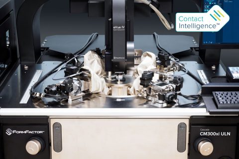
Our transformative approach to the analytical probe systems is specifically designed for this purpose – creating an electrically pristine environment for on-wafer measurements. By eliminating environmental factors that could compromise test results, the prober becomes essentially “invisible” to the measurement instrument. Since the introduction of the first MicroChamber® probe station in 1991, FormFactor’s Cascade probe system products have consistently pursued the same mission – enabling customers to succeed by making informed decisions with the highest quality data.
Delivering Unmatched Experience
FormFactor’s experienced design team has consistently set a higher standard for excellence in electrical measurements. Collaborating closely with our esteemed customers, we’ve achieved a series of innovative breakthroughs that have shaped an extensive line of highly effective technologies. These include, but are not limited to:
- Shielding against EMI/RFI and light interference
- Precise electrical noise filtration
- Strategic signal protection
- Single-point grounding with precision
- Adept noise isolation
- Efficient reduction of contact resistance
- Skillful management of capacitance and inductance, among various other advancements.
These technologies have proven their effectiveness across a wide range of temperatures and in fully automated scenarios, where challenges intensify exponentially.
Our unwavering commitment to preserving the integrity of electrical measurements is a hallmark that distinguishes a FormFactor analytical probe system, ensuring customer success through uncompromised data reliability.