May 24, 2018
Wafer-level electromigration offers three key advantages to a reliability test program compared to PLR: faster time to test results, reduced operating expense, and improved data integrity.

May 24, 2018
Wafer-level electromigration offers three key advantages to a reliability test program compared to PLR: faster time to test results, reduced operating expense, and improved data integrity.
In our last post, we laid out how wafer-level electromigration reduces cycle time for faster feedback. Here, we’ll cover the other two motivating factors for shifting from package-level reliability testing to wafer-level reliability testing: lower cost of ownership and better data integrity.
Wafer-Level Testing Lowers Operating Expense
Cost of ownership is another reason to consider EM WLR. PLR requires the use of expensive, sacrificial ceramic packages for every structure to be tested. In addition to the packages themselves, costs are incurred in the packaging process (whether performed in-house or by a third party) for dicing the wafer, bonding the DUTs into the packages, and shipping wafers and packages; effort is also required to manage the process. These expenses do not abate over time – they continue for the life of the test program, and this accumulates into a significant investment.
EM WLR systems are more expensive per channel in comparison to EM PLR systems. However, this difference in initial investment can eventually be recovered via savings in ongoing package expenses.
Wafer-Level Testing Provides Safer Approach, Better Data Integrity
Reliability margins have shrunk dramatically with recent nodes, rendering simple “worst-case” and one-size-fits-all analysis moot. To massage maximum performance out of each IC element, design rules have become progressively more sophisticated; this demands a broader range of test conditions to check all corner cases and applications and requires ever more accurate data for every case tested.
Data integrity is therefore essential, but DUT packaging comes with multiple damage threats. Sawing the wafer to singulate the test structures uses water, which can be absorbed by the low-k or ultra-low-k dielectric. Worse, multiple opportunities for electrostatic discharge (ESD) damage to DUTs arise during package bonding, shipping, handling, and loading the packages into the system for test.
Water and ESD damage is sometimes immediately apparent (hard-failing DUTs are easily screened out prior to test), but sometimes these can be latent effects which emerge only later during test and which can skew results unpredictably. These issues are especially problematic for technology development when guard rings for protection may not be present but can negatively impact reliability evaluation of mature processes as well.
EM WLR provides a safer approach to test, without EM PLR’s risk of potential data corruption due to moisture absorption and ESD during bonding, shipping, handling, and loading.
To summarize these blog posts, WLR offers three key advantages to a reliability test program compared to PLR: faster time to test results, reduced operating expense, and improved data integrity. With proper equipment capable of high test temperatures up to 350°C and purging oxygen from the test environment, these benefits can even be realized for copper electromigration testing which has long been the domain of PLR. Intrinsic EM WLR test results correlate well with PLR. Therefore, EM WLR can be a very viable and profitable element of a robust and efficient reliability test program.
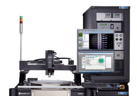
Accelerate your reliability program with electromigration test directly on wafer. Check out our Estrada-EM product line to select the system that will help you discover solutions that immediately enhance accuracy and efficiency.