May 17, 2018
Compressed timelines impels the industry to pursue methods of accelerating design and qualification cycles; utilizing EM WLR to complement EM PLR tangibly enables reliability departments to respond to this challenge.

May 17, 2018
Compressed timelines impels the industry to pursue methods of accelerating design and qualification cycles; utilizing EM WLR to complement EM PLR tangibly enables reliability departments to respond to this challenge.
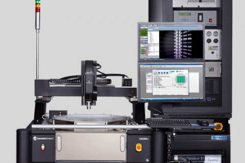
For decades, EM reliability testing has been predominantly performed as a package-level reliability (PLR) activity and has stubbornly remained so even as most other intrinsic reliability tests have shifted toward wafer-level reliability (WLR). Recently, however, this test landscape has changed; robust WLR EM tools are now available to perform this critical reliability test directly on the wafer. The general industry migration from PLR toward WLR has three key motivations:
Let’s explore the first motivation above – faster results. Wafer-Level Testing Reduces Cycle Time for Faster Feedback
Increasing stakes in the technology race apply pressure on reliability labs for quicker answers, and the rising interconnect complexity of new nodes demands investigation of many materials and structure types in a compressed timeframe. This impels the industry to pursue methods of accelerating design and qualification cycles; utilizing EM WLR to complement EM PLR tangibly enables reliability departments to respond to this challenge.
For PLR testing, packaging the devices under test (DUTs) involves sending the wafer to an in-house or external facility to saw and bond the test structures into packages. WLR entirely bypasses this packaging step to test the wafer directly, expediting the test results by days or even weeks as shown in the figure below.

Also shown above, an additional time saving benefit of several days comes from only partially processing the wafer – i.e., building only the metal layers of interest and omitting the finishing steps in order to proceed immediately to test. To take advantage of this opportunity, a WLR system must provide an oxygen-free environment, because the copper pads, lines, and vias on these partially-processed wafers will oxidize very rapidly at EM test temperatures.
Leveraging these schedule improvements can significantly improve a reliability lab’s responsiveness to requests for fast feedback.
The WLR shortcut in the above figure demonstrates how EM WLR can save much of the time necessary to complete EM experiments. However, it should be acknowledged that a smart test program implementation will likely utilize an optimized mix of both methods in a parallel and complimentary fashion:
The improved response times provided by EM WLR are especially valuable during new process development, fab line qualification efforts, adding customer-specific recipes to foundry lines, responding to process excursions, and whenever process tuning is frequent or urgent.
Accelerate your reliability program with electromigration test directly on wafer. Check out our Estrada-EM product line to select the system that will help you discover solutions that immediately enhance accuracy and efficiency.